
A scanning tunneling microscope (STM) is a type of microscope used for imaging surfaces at the atomic level. Its development in 1981 earned its inventors, Gerd Binnig and Heinrich Rohrer, then at IBM Zürich, the Nobel Prize in Physics in 1986. STM senses the surface by using an extremely sharp conducting tip that can distinguish features smaller than 0.1 nm with a 0.01 nm depth resolution. This means that individual atoms can routinely be imaged and manipulated. Most microscopes are built for use in ultra-high vacuum at temperatures approaching zero kelvin, but variants exist for studies in air, water and other environments, and for temperatures over 1000 °C.
Molecular electronics is the study and application of molecular building blocks for the fabrication of electronic components. It is an interdisciplinary area that spans physics, chemistry, and materials science. The unifying feature is use of molecular building blocks to fabricate electronic components. Due to the prospect of size reduction in electronics offered by molecular-level control of properties, molecular electronics has generated much excitement. It provides a potential means to extend Moore's Law beyond the foreseen limits of small-scale conventional silicon integrated circuits.
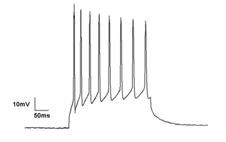
Electrophysiology is the branch of physiology that studies the electrical properties of biological cells and tissues. It involves measurements of voltage changes or electric current or manipulations on a wide variety of scales from single ion channel proteins to whole organs like the heart. In neuroscience, it includes measurements of the electrical activity of neurons, and, in particular, action potential activity. Recordings of large-scale electric signals from the nervous system, such as electroencephalography, may also be referred to as electrophysiological recordings. They are useful for electrodiagnosis and monitoring.

Atomic force microscopy (AFM) or scanning force microscopy (SFM) is a very-high-resolution type of scanning probe microscopy (SPM), with demonstrated resolution on the order of fractions of a nanometer, more than 1000 times better than the optical diffraction limit.
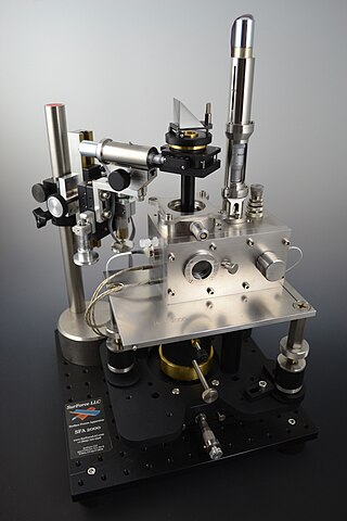
The Surface Force Apparatus (SFA) is a scientific instrument which measures the interaction force of two surfaces as they are brought together and retracted using multiple beam interferometry to monitor surface separation and directly measure contact area and observe any surface deformations occurring in the contact zone. One surface is held by a cantilevered spring, and the deflection of the spring is used to calculate the force being exerted. The technique was pioneered by David Tabor and R.H.S. Winterton in the late 1960s at Cambridge University. By the mid-1970s, J.N. Israelachvili had adapted the original design to operate in liquids, notably aqueous solutions, while at the Australian National University, and further advanced the technique to support friction and electro-chemical surface studies while at the University of California Santa Barbara.
The electrochemical scanning tunneling microscope (EC-STM) is a scanning tunneling microscope that measures the structures of surfaces and electrochemical reactions in solid-liquid interfaces at atomic or molecular scales.
Nanoelectrochemistry is a branch of electrochemistry that investigates the electrical and electrochemical properties of materials at the nanometer size regime. Nanoelectrochemistry plays significant role in the fabrication of various sensors, and devices for detecting molecules at very low concentrations.
A break junction is an electronic device which consists of two metal wires separated by a very thin gap, on the order of the inter-atomic spacing. This can be done by physically pulling the wires apart or through chemical etching or electromigration. As the wire breaks, the separation between the electrodes can be indirectly controlled by monitoring the electrical resistance of the junction.
Inelastic electron tunneling spectroscopy (IETS) is an experimental tool for studying the vibrations of molecular adsorbates on metal oxides. It yields vibrational spectra of the adsorbates with high resolution (< 0.5 meV) and high sensitivity (< 1013 molecules are required to provide a spectrum). An additional advantage is the fact that optically forbidden transitions may be observed as well. Within IETS, an oxide layer with molecules adsorbed on it is put between two metal plates. A bias voltage is applied between the two contacts. An energy diagram of the metal-oxide-metal device under bias is shown in the top figure. The metal contacts are characterized by a constant density of states, filled up to the Fermi energy. The metals are assumed to be equal. The adsorbates are situated on the oxide material. They are represented by a single bridge electronic level, which is the upper dashed line. If the insulator is thin enough, there is a finite probability that the incident electron tunnels through the barrier. Since the energy of the electron is not changed by this process, it is an elastic process. This is shown in the left figure.
Molecular scale electronics, also called single-molecule electronics, is a branch of nanotechnology that uses single molecules, or nanoscale collections of single molecules, as electronic components. Because single molecules constitute the smallest stable structures imaginable, this miniaturization is the ultimate goal for shrinking electrical circuits.
Lipid bilayer characterization is the use of various optical, chemical and physical probing methods to study the properties of lipid bilayers. Many of these techniques are elaborate and require expensive equipment because the fundamental nature of the lipid bilayer makes it a very difficult structure to study. An individual bilayer, since it is only a few nanometers thick, is invisible in traditional light microscopy. The bilayer is also a relatively fragile structure since it is held together entirely by non-covalent bonds and is irreversibly destroyed if removed from water. In spite of these limitations dozens of techniques have been developed over the last seventy years to allow investigations of the structure and function of bilayers. The first general approach was to utilize non-destructive in situ measurements such as x-ray diffraction and electrical resistance which measured bilayer properties but did not actually image the bilayer. Later, protocols were developed to modify the bilayer and allow its direct visualization at first in the electron microscope and, more recently, with fluorescence microscopy. Over the past two decades, a new generation of characterization tools including AFM has allowed the direct probing and imaging of membranes in situ with little to no chemical or physical modification. More recently, dual polarisation interferometry has been used to measure the optical birefringence of lipid bilayers to characterise order and disruption associated with interactions or environmental effects.

Local oxidation nanolithography (LON) is a tip-based nanofabrication method. It is based on the spatial confinement on an oxidation reaction under the sharp tip of an atomic force microscope.
Nanofluidic circuitry is a nanotechnology aiming for control of fluids in nanometer scale. Due to the effect of an electrical double layer within the fluid channel, the behavior of nanofluid is observed to be significantly different compared with its microfluidic counterparts. Its typical characteristic dimensions fall within the range of 1–100 nm. At least one dimension of the structure is in nanoscopic scale. Phenomena of fluids in nano-scale structure are discovered to be of different properties in electrochemistry and fluid dynamics.

Photoconductive atomic force microscopy (PC-AFM) is a variant of atomic force microscopy that measures photoconductivity in addition to surface forces.
Scanning electrochemical microscopy (SECM) is a technique within the broader class of scanning probe microscopy (SPM) that is used to measure the local electrochemical behavior of liquid/solid, liquid/gas and liquid/liquid interfaces. Initial characterization of the technique was credited to University of Texas electrochemist, Allen J. Bard, in 1989. Since then, the theoretical underpinnings have matured to allow widespread use of the technique in chemistry, biology and materials science. Spatially resolved electrochemical signals can be acquired by measuring the current at an ultramicroelectrode (UME) tip as a function of precise tip position over a substrate region of interest. Interpretation of the SECM signal is based on the concept of diffusion-limited current. Two-dimensional raster scan information can be compiled to generate images of surface reactivity and chemical kinetics.

The colloidal probe technique is commonly used to measure interaction forces acting between colloidal particles and/or planar surfaces in air or in solution. This technique relies on the use of an atomic force microscope (AFM). However, instead of a cantilever with a sharp AFM tip, one uses the colloidal probe. The colloidal probe consists of a colloidal particle of few micrometers in diameter that is attached to an AFM cantilever. The colloidal probe technique can be used in the sphere-plane or sphere-sphere geometries. One typically achieves a force resolution between 1 and 100 pN and a distance resolution between 0.5 and 2 nm.

Non-contact atomic force microscopy (nc-AFM), also known as dynamic force microscopy (DFM), is a mode of atomic force microscopy, which itself is a type of scanning probe microscopy. In nc-AFM a sharp probe is moved close to the surface under study, the probe is then raster scanned across the surface, the image is then constructed from the force interactions during the scan. The probe is connected to a resonator, usually a silicon cantilever or a quartz crystal resonator. During measurements the sensor is driven so that it oscillates. The force interactions are measured either by measuring the change in amplitude of the oscillation at a constant frequency just off resonance or by measuring the change in resonant frequency directly using a feedback circuit to always drive the sensor on resonance.
A probe tip is an instrument used in scanning probe microscopes (SPMs) to scan the surface of a sample and make nano-scale images of surfaces and structures. The probe tip is mounted on the end of a cantilever and can be as sharp as a single atom. In microscopy, probe tip geometry and the composition of both the tip and the surface being probed directly affect resolution and imaging quality. Tip size and shape are extremely important in monitoring and detecting interactions between surfaces. SPMs can precisely measure electrostatic forces, magnetic forces, chemical bonding, Van der Waals forces, and capillary forces. SPMs can also reveal the morphology and topography of a surface.

Multi-tip scanning tunneling microscopy extends scanning tunneling microscopy (STM) from imaging to dedicated electrical measurements at the nanoscale like a ″multimeter at the nanoscale″. In materials science, nanoscience, and nanotechnology, it is desirable to measure electrical properties at a particular position of the sample. For this purpose, multi-tip STMs in which several tips are operated independently have been developed. Apart from imaging the sample, the tips of a multi-tip STM are used to form contacts to the sample at desired locations and to perform local electrical measurements.
This glossary of nanotechnology is a list of definitions of terms and concepts relevant to nanotechnology, its sub-disciplines, and related fields.

