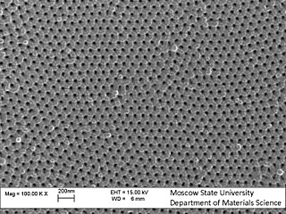
Nanopillars is an emerging technology within the field of nanostructures. Nanopillars are pillar shaped nanostructures approximately 10 nanometers in diameter that can be grouped together in lattice like arrays. [1] They are a type of metamaterial, which means that nanopillars get their attributes from being grouped into artificially designed structures and not their natural properties. Nanopillars set themselves apart from other nanostructures due to their unique shape. Each nanopillar has a pillar shape at the bottom and a tapered pointy end on top. This shape in combination with nanopillars' ability to be grouped together exhibits many useful properties. Nanopillars have many applications including efficient solar panels, high resolution analysis, and antibacterial surfaces.
Due to their tapered ends, nanopillars are very efficient at capturing light. Solar collector surfaces coated with nanopillars are three times as efficient as nanowire solar cells. [2] Less material is needed to build a solar cell out of nanopillars compared to regular semi conductive materials. They also hold up well during the manufacturing process of solar panels. This durability allows manufacturers to use cheaper materials and less expensive methods to produce solar panels. Researchers are looking into putting dopants into the bottom of the nanopillars, [3] to increase the amount of time photons will bounce around the pillars and thus the amount of light captured. As well as capturing light more efficiently, using nanopillars in solar panels will allow them to be flexible. The flexibility gives manufacturers more options on how they want their solar panels to be shaped as well as reduces costs in terms of how delicately the panels have to be handled. [4] Although nanopillars are more efficient and cheaper than standard materials, scientists have not been able to mass-produce them yet. This is a significant drawback to using nanopillars as a part of the manufacturing process.
Nanopillars also have functions outside of electronics and can imitate nature's defenses. Cicadas' wings are covered in tiny, nanopillar shaped rods. When bacteria rests on a cicada's wing, its cell membrane will stick to the nanopillars and the crevices between them, rupturing it. Since the rods on the cicadas are about the same size and shape as artificial nanopillars, it is possible for humans to copy this defense. A surface covered with nanopillars would immediately kill off all soft membrane bacteria. More rigid bacteria will be more likely to not rupture. If mass-produced and installed everywhere, nanopillars could reduce much of the risk of transmitting diseases through touching infected surfaces. [5]
There are several models proposed to explain the antibacterial mechanism of the nanopillars. According to the stretching and mechano-inducing model, [6] for a relatively uniform nanotopographies like nanopillars found on cicada wing, the bacteria die due to the rupturing of bacterial cell wall that is suspended between two adjacent nanopillars as opposed to a puncturing mechanism. The nanopillar features like height, density, and sharpness of the nanopillars was found to be affecting the overall antibacterial properties of the nanopillars. However, the relative correlation of nanopillar features is difficult to establish due to several conflicting results in the literature. [7] Alternative antibacterial mechanism of nanopillars include the potential effects of shear force, [8] negative physiological response of bacteria, [9] and intrinsic pressure effects from the interaction between bacterial surface proteins and nanopillars. [10]
Another use of nanopillars is observing cells. Nanopillars capture light so well that when lights hits them, the glow the nanopillars emit dies down at around 150 nanometers. Because this distance is less than the wavelength of light, it allows researchers to observe small objects without the interference of background light. [11] This is especially useful in cellular analysis. The cells group around the nanopillars because of its small size and recognize it as an organelle. [12] The nanopillars simply hold the cells in place while the cells are being observed.
In 2006, researchers at the University of Nebraska-Lincoln and the Lawrence Livermore National Laboratory developed a cheaper and more efficient way to create nanopillars. They used a combination of nanosphere lithography (a way of organizing the lattice) and reactive ion etching(molding the nanopillars to the right shape) to make large groups of silicon pillars with less than 500 nm diameters. [13] Then, in 2010, researchers fabricated a way to manufacture nanopillars with tapered ends. [14] The former design of a pillar with a flat blunt top reflected much of the light coming onto the pillars. The tapered tops allow light to enter the forest of nanopillars and the wider bottom absorbs almost all of the light that hits it. This design captures about 99% of the light whereas nanorods which have a uniform thickness only captured 85% of the light. After the introduction of tapered ends, researchers started to find many more applications for nanopillars.
Constructing nanopillars is a simple but lengthy procedure that can take hours. [15] The process to create nanopillars starts with anodizing a 2.5 mm thick aluminum foil mold. Anodizing the foil creates pores in the foil a micrometer deep and 60 nanometers wide. The next step is to treat the foil with phosphoric acid which expands the pores to 130 nanometers. The foil is anodized once more making its pores a micrometer deeper. Lastly, a small amount of gold is added to the pores to catalyze the reaction for the growth of the semiconductor material. When the aluminum is scraped away there is a forest of nanopillars left inside a casing of aluminum oxide. [16] Furthermore, pillar and tube structures can also be fabricated by the top-down approach of the combination of deep UV (DUV) lithography and atomic layer deposition (ALD). [17] [18]
A bactericide or bacteriocide, sometimes abbreviated Bcidal, is a substance which kills bacteria. Bactericides are disinfectants, antiseptics, or antibiotics. However, material surfaces can also have bactericidal properties based solely on their physical surface structure, as for example biomaterials like insect wings.
Peptidoglycan or murein is a unique large macromolecule, a polysaccharide, consisting of sugars and amino acids that forms a mesh-like peptidoglycan layer outside the plasma membrane, the rigid cell wall characteristic of most bacteria. The sugar component consists of alternating residues of β-(1,4) linked N-acetylglucosamine (NAG) and N-acetylmuramic acid (NAM). Attached to the N-acetylmuramic acid is a oligopeptide chain made of three to five amino acids. The peptide chain can be cross-linked to the peptide chain of another strand forming the 3D mesh-like layer. Peptidoglycan serves a structural role in the bacterial cell wall, giving structural strength, as well as counteracting the osmotic pressure of the cytoplasm. This repetitive linking results in a dense peptidoglycan layer which is critical for maintaining cell form and withstanding high osmotic pressures, and it is regularly replaced by peptidoglycan production. Peptidoglycan hydrolysis and synthesis are two processes that must occur in order for cells to grow and multiply, a technique carried out in three stages: clipping of current material, insertion of new material, and re-crosslinking of existing material to new material.

Molecular engineering is an emerging field of study concerned with the design and testing of molecular properties, behavior and interactions in order to assemble better materials, systems, and processes for specific functions. This approach, in which observable properties of a macroscopic system are influenced by direct alteration of a molecular structure, falls into the broader category of “bottom-up” design.
A "photoelectrochemical cell" is one of two distinct classes of device. The first produces electrical energy similarly to a dye-sensitized photovoltaic cell, which meets the standard definition of a photovoltaic cell. The second is a photoelectrolytic cell, that is, a device which uses light incident on a photosensitizer, semiconductor, or aqueous metal immersed in an electrolytic solution to directly cause a chemical reaction, for example to produce hydrogen via the electrolysis of water.

A dye-sensitized solar cell is a low-cost solar cell belonging to the group of thin film solar cells. It is based on a semiconductor formed between a photo-sensitized anode and an electrolyte, a photoelectrochemical system. The modern version of a dye solar cell, also known as the Grätzel cell, was originally co-invented in 1988 by Brian O'Regan and Michael Grätzel at UC Berkeley and this work was later developed by the aforementioned scientists at the École Polytechnique Fédérale de Lausanne (EPFL) until the publication of the first high efficiency DSSC in 1991. Michael Grätzel has been awarded the 2010 Millennium Technology Prize for this invention.

A solar cell, or photovoltaic cell, is an electronic device that converts the energy of light directly into electricity by the photovoltaic effect, which is a physical and chemical phenomenon. It is a form of photoelectric cell, defined as a device whose electrical characteristics, such as current, voltage, or resistance, vary when exposed to light. Individual solar cell devices are often the electrical building blocks of photovoltaic modules, known colloquially as solar panels. The common single junction silicon solar cell can produce a maximum open-circuit voltage of approximately 0.5 volts to 0.6volts.
Porous silicon is a form of the chemical element silicon that has introduced nanopores in its microstructure, rendering a large surface to volume ratio in the order of 500 m2/cm3.
Hybrid solar cells combine advantages of both organic and inorganic semiconductors. Hybrid photovoltaics have organic materials that consist of conjugated polymers that absorb light as the donor and transport holes. Inorganic materials in hybrid cells are used as the acceptor and electron transporter in the structure. The hybrid photovoltaic devices have a potential for not only low-cost by roll-to-roll processing but also for scalable solar power conversion.
Nanophotonics or nano-optics is the study of the behavior of light on the nanometer scale, and of the interaction of nanometer-scale objects with light. It is a branch of optics, optical engineering, electrical engineering, and nanotechnology. It often involves dielectric structures such as nanoantennas, or metallic components, which can transport and focus light via surface plasmon polaritons.
Nanofoams are a class of nanostructured, porous materials (foams) containing a significant population of pores with diameters less than 100 nm. Aerogels are one example of nanofoam.

Nanobatteries are fabricated batteries employing technology at the nanoscale, particles that measure less than 100 nanometers or 10−7 meters. These batteries may be nano in size or may use nanotechnology in a macro scale battery. Nanoscale batteries can be combined to function as a macrobattery such as within a nanopore battery.
Green nanotechnology refers to the use of nanotechnology to enhance the environmental sustainability of processes producing negative externalities. It also refers to the use of the products of nanotechnology to enhance sustainability. It includes making green nano-products and using nano-products in support of sustainability.
Black silicon is a semiconductor material, a surface modification of silicon with very low reflectivity and correspondingly high absorption of visible light.
A plasmonic-enhanced solar cell, commonly referred to simply as plasmonic solar cell, is a type of solar cell that converts light into electricity with the assistance of plasmons, but where the photovoltaic effect occurs in another material.
Nanocrystal solar cells are solar cells based on a substrate with a coating of nanocrystals. The nanocrystals are typically based on silicon, CdTe or CIGS and the substrates are generally silicon or various organic conductors. Quantum dot solar cells are a variant of this approach, but take advantage of quantum mechanical effects to extract further performance. Dye-sensitized solar cells are another related approach, but in this case the nano-structuring is part of the substrate.
Anodic aluminium oxide, anodic aluminum oxide (AAO), or anodic alumina is a self-organized form of aluminium oxide that has a honeycomb-like structure formed by high density arrays of uniform and parallel pores. The diameter of the pores can be as low as 5 nanometers and as high as several hundred nanometers, and length can be controlled from few tens of nanometers to few hundred micrometers. Porous AAO is formed by electrochemical oxidation (anodization) of aluminum in acid electrolytes in the conditions that balance the growth and the AAO films are formed with limited thickness.
Ion tracks are damage-trails created by swift heavy ions penetrating through solids, which may be sufficiently-contiguous for chemical etching in a variety of crystalline, glassy, and/or polymeric solids. They are associated with cylindrical damage-regions several nanometers in diameter and can be studied by Rutherford backscattering spectrometry (RBS), transmission electron microscopy (TEM), small-angle neutron scattering (SANS), small-angle X-ray scattering (SAXS) or gas permeation.
Nanotopography refers to specific surface features which form or are generated at the nanoscopic scale. While the term can be used to describe a broad range of applications ranging from integrated circuits to microfluidics, in practice it typically applied to sub-micron textured surfaces as used in biomaterials research.
Nanosponges are a type of nanoparticle, often a synthesized carbon-containing polymer. They are porous in structure, pores being about 1–2 nanometers in size, and can therefore be targeted to absorb small amounts of matter or toxin. Nanosponges are often used in medicine as targeted drug delivery systems, detoxification methods, or as a way of damage control after an injury. They can also be used in environmental applications to clean up ecosystems by performing tasks like purifying water or metal deposits. Their small size allows them to move quickly through substances, like water or blood, efficiently finding and attacking unwanted matter. Nanosponges are often synthetically manufactured but oftentimes include natural materials to improve their efficiency when injected into the body. Nanosponges are superior to microsponges in application as the smaller size allows less disruption into the system in which it is implemented therefore imposing less risk of failed or detrimental effects. The prefix "nano" implies that items of this size are measured on a scale of meters.
Silicon nanowires, also referred to as SiNWs, are a type of semiconductor nanowire most often formed from a silicon precursor by etching of a solid or through catalyzed growth from a vapor or liquid phase. Such nanowires have promising applications in lithium ion batteries, thermoelectrics and sensors. Initial synthesis of SiNWs is often accompanied by thermal oxidation steps to yield structures of accurately tailored size and morphology.