
An integrated circuit or monolithic integrated circuit is a set of electronic circuits on one small flat piece of semiconductor material that is normally silicon. The integration of large numbers of tiny MOS transistors into a small chip results in circuits that are orders of magnitude smaller, faster, and less expensive than those constructed of discrete electronic components. The IC's mass production capability, reliability, and building-block approach to integrated circuit design has ensured the rapid adoption of standardized ICs in place of designs using discrete transistors. ICs are now used in virtually all electronic equipment and have revolutionized the world of electronics. Computers, mobile phones, and other digital home appliances are now inextricable parts of the structure of modern societies, made possible by the small size and low cost of ICs.
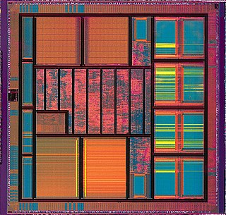
Very large-scale integration (VLSI) is the process of creating an integrated circuit (IC) by combining millions of MOS transistors onto a single chip. VLSI began in the 1970s when MOS integrated circuit chips were widely adopted, enabling complex semiconductor and telecommunication technologies to be developed. The microprocessor and memory chips are VLSI devices. Before the introduction of VLSI technology, most ICs had a limited set of functions they could perform. An electronic circuit might consist of a CPU, ROM, RAM and other glue logic. VLSI lets IC designers add all of these into one chip.
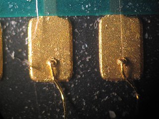
Wire bonding is the method of making interconnections between an integrated circuit (IC) or other semiconductor device and its packaging during semiconductor device fabrication. Although less common, wire bonding can be used to connect an IC to other electronics or to connect from one printed circuit board (PCB) to another. Wire bonding is generally considered the most cost-effective and flexible interconnect technology and is used to assemble the vast majority of semiconductor packages. Wire bonding can be used at frequencies above 100 GHz.

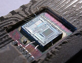
In electronics manufacturing, integrated circuit packaging is the final stage of semiconductor device fabrication, in which the block of semiconductor material is encapsulated in a supporting case that prevents physical damage and corrosion. The case, known as a "package", supports the electrical contacts which connect the device to a circuit board.

Electromigration is the transport of material caused by the gradual movement of the ions in a conductor due to the momentum transfer between conducting electrons and diffusing metal atoms. The effect is important in applications where high direct current densities are used, such as in microelectronics and related structures. As the structure size in electronics such as integrated circuits (ICs) decreases, the practical significance of this effect increases.

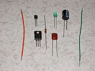
An electronic component is any basic discrete device or physical entity in an electronic system used to affect electrons or their associated fields. Electronic components are mostly industrial products, available in a singular form and are not to be confused with electrical elements, which are conceptual abstractions representing idealized electronic components.
In electronics, a lead is an electrical connection consisting of a length of wire or a metal pad that is designed to connect two locations electrically. Leads are used for many purposes, including: transfer of power; testing of an electrical circuit to see if it is working, using a test light or a multimeter; transmitting information, as when the leads from an electrocardiograph are attached to a person's body to transmit information about their heart rhythm; and sometimes to act as a heatsink. The tiny leads coming off through-hole electronic components are also often called "pins"; in ball grid array packages, they are in form of small spheres, and are therefore called "balls".

The back end of line (BEOL) is the second portion of IC fabrication where the individual devices get interconnected with wiring on the wafer, the metalization layer. Common metals are copper and aluminum. BEOL generally begins when the first layer of metal is deposited on the wafer. BEOL includes contacts, insulating layers (dielectrics), metal levels, and bonding sites for chip-to-package connections.

A multi-chip module (MCM) is generically an electronic assembly where multiple integrated circuits, semiconductor dies and/or other discrete components are integrated, usually onto a unifying substrate, so that in use it can be treated as if it were a larger IC. Other terms, such as "hybrid" or "hybrid integrated circuit", also refer to MCMs. The individual ICs that make up an MCM are known as chiplets. Intel and AMD are using MCMs to improve performance and reduce costs, as splitting a large monolithic IC into smaller chiplets allows for easy performance improvements, more ICs per wafer, and improved yield, as smaller dies have a reduced risk of getting destroyed by process variations during semiconductor fabrication. This approach also allows for chiplets to be reused in several products, reduces the amount of time required to design a module compared to designing a monolithic IC, and also reduces the number of bugs that have to be solved during design. However, communication between chiplets consumes more power and has higher latency than components in monolithic ICs. Each chiplet is physically smaller than a conventional monolithic IC die,. An example of MCMs in use for mainstream CPUs is AMD's Zen 2 design.

Integrated circuit design, or IC design, is a subset of electronics engineering, encompassing the particular logic and circuit design techniques required to design integrated circuits, or ICs. ICs consist of miniaturized electronic components built into an electrical network on a monolithic semiconductor substrate by photolithography.

Signal integrity or SI is a set of measures of the quality of an electrical signal. In digital electronics, a stream of binary values is represented by a voltage waveform. However, digital signals are fundamentally analog in nature, and all signals are subject to effects such as noise, distortion, and loss. Over short distances and at low bit rates, a simple conductor can transmit this with sufficient fidelity. At high bit rates and over longer distances or through various mediums, various effects can degrade the electrical signal to the point where errors occur and the system or device fails. Signal integrity engineering is the task of analyzing and mitigating these effects. It is an important activity at all levels of electronics packaging and assembly, from internal connections of an integrated circuit (IC), through the package, the printed circuit board (PCB), the backplane, and inter-system connections. While there are some common themes at these various levels, there are also practical considerations, in particular the interconnect flight time versus the bit period, that cause substantial differences in the approach to signal integrity for on-chip connections versus chip-to-chip connections.
In an integrated circuit, a signal can couple from one node to another via the substrate. This phenomenon is referred to as substrate coupling or substrate noise coupling.
The interconnect bottleneck comprises limits on integrated circuit (IC) performance due to connections between components instead of their internal speed. In 2006 it was predicted to be a "looming crisis" by 2010.
In integrated circuits, electrical power is distributed to the components of the chip over a network of conductors on the chip. Power network design includes the analysis and design of such networks. As in all engineering, this involves tradeoffs - the network must have adequate performance, be sufficiently reliable, but should not use more resources than required.
An electronic circuit is composed of individual electronic components, such as resistors, transistors, capacitors, inductors and diodes, connected by conductive wires or traces through which electric current can flow. To be referred to as electronic, rather than electrical, generally at least one active component must be present. The combination of components and wires allows various simple and complex operations to be performed: signals can be amplified, computations can be performed, and data can be moved from one place to another.

In electronic engineering, a through-silicon via (TSV) or through-chip via is a vertical electrical connection (via) that passes completely through a silicon wafer or die. TSVs are high-performance interconnect techniques used as an alternative to wire-bond and flip chips to create 3D packages and 3D integrated circuits. Compared to alternatives such as package-on-package, the interconnect and device density is substantially higher, and the length of the connections becomes shorter.
A three-dimensional integrated circuit is a MOS integrated circuit (IC) manufactured by stacking silicon wafers or dies and interconnecting them vertically using, for instance, through-silicon vias (TSVs) or Cu-Cu connections, so that they behave as a single device to achieve performance improvements at reduced power and smaller footprint than conventional two dimensional processes. The 3D IC is one of several 3D integration schemes that exploit the z-direction to achieve electrical performance benefits in microelectronics and nanoelectronics.
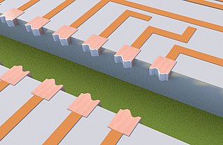
Quilt Packaging (QP) is an integrated circuit packaging and chip-to-chip interconnect packaging technology that utilizes “nodule” structures that extend out horizontally from the edges of microchips to make electrically and mechanically robust chip-to-chip interconnections.
In integrated circuits (ICs), interconnects are structures that connect two or more circuit elements together electrically. The design and layout of interconnects on an IC is vital to its proper function, performance, power efficiency, reliability, and fabrication yield. The material interconnects are made from depends on many factors. Chemical and mechanical compatibility with the semiconductor substrate, and the dielectric in between the levels of interconnect is necessary, otherwise barrier layers are needed. Suitability for fabrication is also required; some chemistries and processes prevent integration of materials and unit processes into a larger technology (recipe) for IC fabrication. In fabrication, interconnects are formed during the back-end-of-line after the fabrication of the transistors on the substrate.
Glossary of Microelectronics Manufacturing Terms