
Chemical vapor deposition (CVD) is a vacuum deposition method used to produce high-quality, and high-performance, solid materials. The process is often used in the semiconductor industry to produce thin films.
A thin film is a layer of material ranging from fractions of a nanometer (monolayer) to several micrometers in thickness. The controlled synthesis of materials as thin films is a fundamental step in many applications. A familiar example is the household mirror, which typically has a thin metal coating on the back of a sheet of glass to form a reflective interface. The process of silvering was once commonly used to produce mirrors, while more recently the metal layer is deposited using techniques such as sputtering. Advances in thin film deposition techniques during the 20th century have enabled a wide range of technological breakthroughs in areas such as magnetic recording media, electronic semiconductor devices, integrated passive devices, LEDs, optical coatings, hard coatings on cutting tools, and for both energy generation and storage. It is also being applied to pharmaceuticals, via thin-film drug delivery. A stack of thin films is called a multilayer.
Titanium nitride is an extremely hard ceramic material, often used as a physical vapor deposition (PVD) coating on titanium alloys, steel, carbide, and aluminium components to improve the substrate's surface properties.

Zirconium nitride is an inorganic compound used in a variety of ways due to its properties.
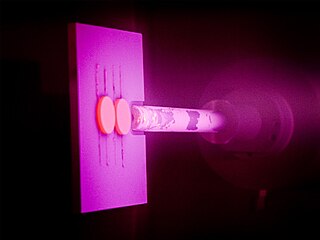
Cathodic arc deposition or Arc-PVD is a physical vapor deposition technique in which an electric arc is used to vaporize material from a cathode target. The vaporized material then condenses on a substrate, forming a thin film. The technique can be used to deposit metallic, ceramic, and composite films.

Ion plating (IP) is a physical vapor deposition (PVD) process that is sometimes called ion assisted deposition (IAD) or ion vapor deposition (IVD) and is a modified version of vacuum deposition. Ion plating uses concurrent or periodic bombardment of the substrate, and deposits film by atomic-sized energetic particles called ions. Bombardment prior to deposition is used to sputter clean the substrate surface. During deposition the bombardment is used to modify and control the properties of the depositing film. It is important that the bombardment be continuous between the cleaning and the deposition portions of the process to maintain an atomically clean interface. If this interface is not properly cleaned, then it can result into a weaker coating or poor adhesion.

Microfabrication is the process of fabricating miniature structures of micrometre scales and smaller. Historically, the earliest microfabrication processes were used for integrated circuit fabrication, also known as "semiconductor manufacturing" or "semiconductor device fabrication". In the last two decades microelectromechanical systems (MEMS), microsystems, micromachines and their subfields, microfluidics/lab-on-a-chip, optical MEMS, RF MEMS, PowerMEMS, BioMEMS and their extension into nanoscale have re-used, adapted or extended microfabrication methods. Flat-panel displays and solar cells are also using similar techniques.
Atomic layer deposition (ALD) is a thin-film deposition technique based on the sequential use of a gas-phase chemical process; it is a subclass of chemical vapour deposition. The majority of ALD reactions use two chemicals called precursors. These precursors react with the surface of a material one at a time in a sequential, self-limiting, manner. A thin film is slowly deposited through repeated exposure to separate precursors. ALD is a key process in fabricating semiconductor devices, and part of the set of tools for synthesizing nanomaterials.

Parylene is the common name of a polymer whose backbone consists of para-benzenediyl rings –C
6H
4– connected by 1,2-ethanediyl bridges –CH
2–CH
2–. It can be obtained by polymerization of para-xylyleneH
2C=C
6H
4=CH
2.
Electron-beam physical vapor deposition, or EBPVD, is a form of physical vapor deposition in which a target anode is bombarded with an electron beam given off by a charged tungsten filament under high vacuum. The electron beam causes atoms from the target to transform into the gaseous phase. These atoms then precipitate into solid form, coating everything in the vacuum chamber with a thin layer of the anode material.
Micromy is a hard surface coating company based in Täby, Sweden. The company specializes in applying hard coating to a wide range of substrate materials using a PVD process. Depending on the application, different coating film materials can be produced, such as TiN, TiC, TiNC, AlTiN or DLC. The coating is mainly used for industrial applications based on the different properties of the materials. However, the PVD process results in a finish such that many coatings are equally suitable for decorative purposes.

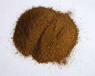
Tantalum nitride (TaN) is a chemical compound, a nitride of tantalum. There are multiple phases of compounds, stoichimetrically from Ta2N to Ta3N5, including TaN.
Vacuum deposition is a group of processes used to deposit layers of material atom-by-atom or molecule-by-molecule on a solid surface. These processes operate at pressures well below atmospheric pressure. The deposited layers can range from a thickness of one atom up to millimeters, forming freestanding structures. Multiple layers of different materials can be used, for example to form optical coatings. The process can be qualified based on the vapor source; physical vapor deposition uses a liquid or solid source and chemical vapor deposition uses a chemical vapor.
Physical vapor deposition (PVD), sometimes called physical vapor transport (PVT), describes a variety of vacuum deposition methods which can be used to produce thin films and coatings on substrates including metals, ceramics, glass, and polymers. PVD is characterized by a process in which the material transitions from a condensed phase to a vapor phase and then back to a thin film condensed phase. The most common PVD processes are sputtering and evaporation. PVD is used in the manufacturing of items which require thin films for optical, mechanical, electrical, acoustic or chemical functions. Examples include semiconductor devices such as thin-film solar cells, microelectromechanical devices such as thin film bulk acoustic resonator, aluminized PET film for food packaging and balloons, and titanium nitride coated cutting tools for metalworking. Besides PVD tools for fabrication, special smaller tools used mainly for scientific purposes have been developed.
Carbon films are thin film coatings which consist predominantly of the chemical element carbon. They include plasma polymer films, amorphous carbon films, CVD diamond films as well as graphite films.

Sputter deposition is a physical vapor deposition (PVD) method of thin film deposition by the phenomenon of sputtering. This involves ejecting material from a "target" that is a source onto a "substrate" such as a silicon wafer. Resputtering is re-emission of the deposited material during the deposition process by ion or atom bombardment. Sputtered atoms ejected from the target have a wide energy distribution, typically up to tens of eV. The sputtered ions can ballistically fly from the target in straight lines and impact energetically on the substrates or vacuum chamber. Alternatively, at higher gas pressures, the ions collide with the gas atoms that act as a moderator and move diffusively, reaching the substrates or vacuum chamber wall and condensing after undergoing a random walk. The entire range from high-energy ballistic impact to low-energy thermalized motion is accessible by changing the background gas pressure. The sputtering gas is often an inert gas such as argon. For efficient momentum transfer, the atomic weight of the sputtering gas should be close to the atomic weight of the target, so for sputtering light elements neon is preferable, while for heavy elements krypton or xenon are used. Reactive gases can also be used to sputter compounds. The compound can be formed on the target surface, in-flight or on the substrate depending on the process parameters. The availability of many parameters that control sputter deposition make it a complex process, but also allow experts a large degree of control over the growth and microstructure of the film.
High-power impulse magnetron sputtering is a method for physical vapor deposition of thin films which is based on magnetron sputter deposition. HIPIMS utilises extremely high power densities of the order of kW⋅cm−2 in short pulses (impulses) of tens of microseconds at low duty cycle of < 10%. Distinguishing features of HIPIMS are a high degree of ionisation of the sputtered metal and a high rate of molecular gas dissociation which result in high density of deposited films. The ionization and dissociation degree increase according to the peak cathode power. The limit is determined by the transition of the discharge from glow to arc phase. The peak power and the duty cycle are selected so as to maintain an average cathode power similar to conventional sputtering (1–10 W⋅cm−2).
Metallised films are polymer films coated with a thin layer of metal, usually aluminium. They offer the glossy metallic appearance of an aluminium foil at a reduced weight and cost. Metallised films are widely used for decorative purposes and food packaging, and also for specialty applications including insulation and electronics.
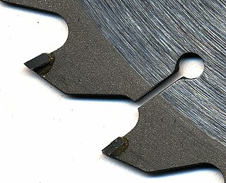
Cemented carbides are a class of hard materials used extensively for cutting tools, as well as in other industrial applications. It consists of fine particles of carbide cemented into a composite by a binder metal. Cemented carbides commonly use tungsten carbide (WC), titanium carbide (TiC), or tantalum carbide (TaC) as the aggregate. Mentions of "carbide" or "tungsten carbide" in industrial contexts usually refer to these cemented composites.

Titanium aluminium nitride (TiAlN) or aluminium titanium nitride is a group of metastable hard coatings consisting of nitrogen and the metallic elements aluminium and titanium. This compound as well as similar compounds(such as TiN and TiCN) are most notably used for coating machine tools such and endmills and drills to change their properties, such as increased thermal stability and/or wear resistance. Four important compositions are deposited in industrial scale by physical vapor deposition methods: