
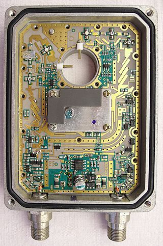
A printed circuit board (PCB), also called printed wiring board (PWB), is a laminated sandwich structure of conductive and insulating layers, each with a pattern of traces, planes and other features etched from one or more sheet layers of copper laminated onto or between sheet layers of a non-conductive substrate. PCBs are used to connect or "wire" components to one another in an electronic circuit. Electrical components may be fixed to conductive pads on the outer layers, generally by soldering, which both electrically connects and mechanically fastens the components to the board. Another manufacturing process adds vias, metal-lined drilled holes that enable electrical interconnections between conductive layers, to boards with more than a single side.
In telecommunication, a microstrip antenna usually is an antenna fabricated using photolithographic techniques on a printed circuit board (PCB). It is a kind of internal antenna. They are mostly used at microwave frequencies. An individual microstrip antenna consists of a patch of metal foil of various shapes on the surface of a PCB, with a metal foil ground plane on the other side of the board. Most microstrip antennas consist of multiple patches in a two-dimensional array. The antenna is usually connected to the transmitter or receiver through foil microstrip transmission lines. The radio frequency current is applied between the antenna and ground plane. Microstrip antennas have become very popular in recent decades due to their thin planar profile which can be incorporated into the surfaces of consumer products, aircraft and missiles; their ease of fabrication using printed circuit techniques; the ease of integrating the antenna on the same board with the rest of the circuit, and the possibility of adding active devices such as microwave integrated circuits to the antenna itself to make active antennas Patch antenna. Based on its origin, microstrip consists of two words, namely micro and is defined as a type of antenna that has a blade/piece shape and is very thin/small.
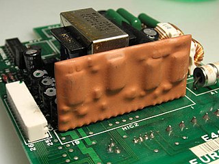
A hybrid integrated circuit (HIC), hybrid microcircuit, hybrid circuit or simply hybrid is a miniaturized electronic circuit constructed of individual devices, such as semiconductor devices and passive components, bonded to a substrate or printed circuit board (PCB). A PCB having components on a Printed wiring board (PWB) is not considered a true hybrid circuit according to the definition of MIL-PRF-38534.
In telecommunications and electrical engineering in general, an unbalanced line is a pair of conductors intended to carry electrical signals, which have unequal impedances along their lengths and to ground and other circuits. Examples of unbalanced lines are coaxial cable or the historic earth return system invented for the telegraph, but rarely used today. Unbalanced lines are to be contrasted with balanced lines, such as twin-lead or twisted pair which use two identical conductors to maintain impedance balance throughout the line. Balanced and unbalanced lines can be interfaced using a device called a balun.
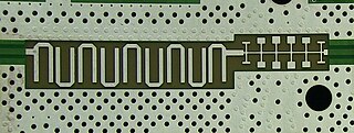
The spurline is a type of radio-frequency and microwave distributed element filter with band-stop (notch) characteristics, most commonly used with microstrip transmission lines. Spurlines usually exhibit moderate to narrow-band rejection, at about 10% around the central frequency.
In electronics, stripline is a transverse electromagnetic (TEM) transmission line medium invented by Robert M. Barrett of the Air Force Cambridge Research Centre in the 1950s. Stripline is the earliest form of planar transmission line.
The role of the substrate in power electronics is to provide the interconnections to form an electric circuit, and to cool the components. Compared to materials and techniques used in lower power microelectronics, these substrates must carry higher currents and provide a higher voltage isolation. They also must operate over a wide temperature range.
Radio frequency (RF) and microwave filters represent a class of electronic filter, designed to operate on signals in the megahertz to gigahertz frequency ranges. It is component that is used in electronic systems to pass or reject specific frequencies and attenuate of unwanted signals within the microwave and RF range. This frequency range is the range used by most broadcast radio, television, wireless communication, and thus most RF and microwave devices will include some kind of filtering on the signals transmitted or received. Such filters are commonly used as building blocks for duplexers and diplexers to combine or separate multiple frequency bands.

A radio-frequency microelectromechanical system is a microelectromechanical system with electronic components comprising moving sub-millimeter-sized parts that provide radio-frequency (RF) functionality. RF functionality can be implemented using a variety of RF technologies. Besides RF MEMS technology, III-V compound semiconductor, ferrite, ferroelectric, silicon-based semiconductor, and vacuum tube technology are available to the RF designer. Each of the RF technologies offers a distinct trade-off between cost, frequency, gain, large-scale integration, lifetime, linearity, noise figure, packaging, power handling, power consumption, reliability, ruggedness, size, supply voltage, switching time and weight.

Integrated passive devices (IPDs), also known as integrated passive components (IPCs) or embedded passive components (EPC), are electronic components where resistors (R), capacitors (C), inductors (L)/coils/chokes, microstriplines, impedance matching elements, baluns or any combinations of them are integrated in the same package or on the same substrate. Sometimes integrated passives can also be called as embedded passives, and still the difference between integrated and embedded passives is technically unclear. In both cases passives are realized in between dielectric layers or on the same substrate.
A distributed-element filter is an electronic filter in which capacitance, inductance, and resistance are not localised in discrete capacitors, inductors, and resistors as they are in conventional filters. Its purpose is to allow a range of signal frequencies to pass, but to block others. Conventional filters are constructed from inductors and capacitors, and the circuits so built are described by the lumped element model, which considers each element to be "lumped together" at one place. That model is conceptually simple, but it becomes increasingly unreliable as the frequency of the signal increases, or equivalently as the wavelength decreases. The distributed-element model applies at all frequencies, and is used in transmission-line theory; many distributed-element components are made of short lengths of transmission line. In the distributed view of circuits, the elements are distributed along the length of conductors and are inextricably mixed together. The filter design is usually concerned only with inductance and capacitance, but because of this mixing of elements they cannot be treated as separate "lumped" capacitors and inductors. There is no precise frequency above which distributed element filters must be used but they are especially associated with the microwave band.

Metamaterial antennas are a class of antennas which use metamaterials to increase performance of miniaturized antenna systems. Their purpose, as with any electromagnetic antenna, is to launch energy into free space. However, this class of antenna incorporates metamaterials, which are materials engineered with novel, often microscopic, structures to produce unusual physical properties. Antenna designs incorporating metamaterials can step-up the antenna's radiated power.

A waveguide filter is an electronic filter constructed with waveguide technology. Waveguides are hollow metal conduits inside which an electromagnetic wave may be transmitted. Filters are devices used to allow signals at some frequencies to pass, while others are rejected. Filters are a basic component of electronic engineering designs and have numerous applications. These include selection of signals and limitation of noise. Waveguide filters are most useful in the microwave band of frequencies, where they are a convenient size and have low loss. Examples of microwave filter use are found in satellite communications, telephone networks, and television broadcasting.

A substrate-integrated waveguide (SIW) is a synthetic rectangular electromagnetic waveguide formed in a dielectric substrate by densely arraying metallized posts or via holes that connect the upper and lower metal plates of the substrate. The waveguide can be easily fabricated with low-cost mass-production using through-hole techniques, where the post walls consists of via fences. SIW is known to have similar guided wave and mode characteristics to conventional rectangular waveguide with equivalent guide wavelength.
A via fence, also called a picket fence, is a structure used in planar electronic circuit technologies to improve isolation between components that would otherwise be coupled by electromagnetic fields. It consists of a row of via holes which, if spaced close enough together, form a barrier to electromagnetic wave propagation of slab modes in the substrate. Additionally if radiation in the air above the board is also to be suppressed, then a strip pad with via fence allows a shielding can to be electrically attached to the top side, but electrically behave as if it continued through the PCB.
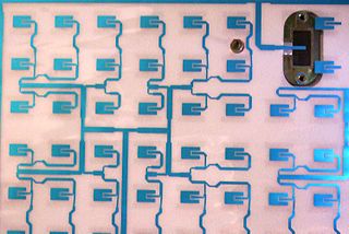
Planar transmission lines are transmission lines with conductors, or in some cases dielectric (insulating) strips, that are flat, ribbon-shaped lines. They are used to interconnect components on printed circuits and integrated circuits working at microwave frequencies because the planar type fits in well with the manufacturing methods for these components. Transmission lines are more than simply interconnections. With simple interconnections, the propagation of the electromagnetic wave along the wire is fast enough to be considered instantaneous, and the voltages at each end of the wire can be considered identical. If the wire is longer than a large fraction of a wavelength, these assumptions are no longer true and transmission line theory must be used instead. With transmission lines, the geometry of the line is precisely controlled so that its electrical behaviour is highly predictable. At lower frequencies, these considerations are only necessary for the cables connecting different pieces of equipment, but at microwave frequencies the distance at which transmission line theory becomes necessary is measured in millimetres. Hence, transmission lines are needed within circuits.
Coplanar waveguide is a type of electrical planar transmission line which can be fabricated using printed circuit board technology, and is used to convey microwave-frequency signals. On a smaller scale, coplanar waveguide transmission lines are also built into monolithic microwave integrated circuits.

Co-fired ceramic devices are monolithic, ceramic microelectronic devices where the entire ceramic support structure and any conductive, resistive, and dielectric materials are fired in a kiln at the same time. Typical devices include capacitors, inductors, resistors, transformers, and hybrid circuits. The technology is also used for robust assembly and packaging of electronic components multi-layer packaging in the electronics industry, such as military electronics, MEMS, microprocessor and RF applications.
Air stripline is a form of electrical planar transmission line whereby a conductor in the form of a thin metal strip is suspended between two ground planes. The idea is to make the dielectric essentially air. Mechanical support of the line may be a thin substrate, periodical insulated supports, or the device connectors and other electrical items.

Distributed-element circuits are electrical circuits composed of lengths of transmission lines or other distributed components. These circuits perform the same functions as conventional circuits composed of passive components, such as capacitors, inductors, and transformers. They are used mostly at microwave frequencies, where conventional components are difficult to implement.

