Related Research Articles
Photolithography is a process used in the manufacturing of integrated circuits. It involves using light to transfer a pattern onto a substrate, typically a silicon wafer.

Screen printing is a printing technique where a mesh is used to transfer ink onto a substrate, except in areas made impermeable to the ink by a blocking stencil. A blade or squeegee is moved across the screen to fill the open mesh apertures with ink, and a reverse stroke then causes the screen to touch the substrate momentarily along a line of contact. This causes the ink to wet the substrate and be pulled out of the mesh apertures as the screen springs back after the blade has passed. One colour is printed at a time, so several screens can be used to produce a multi-coloured image or design.

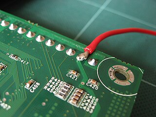
A printed circuit board (PCB), also called printed wiring board (PWB), is a medium used to connect or "wire" components to one another in a circuit. It takes the form of a laminated sandwich structure of conductive and insulating layers: each of the conductive layers is designed with a pattern of traces, planes and other features etched from one or more sheet layers of copper laminated onto and/or between sheet layers of a non-conductive substrate. Electrical components may be fixed to conductive pads on the outer layers in the shape designed to accept the component's terminals, generally by means of soldering, to both electrically connect and mechanically fasten them to it. Another manufacturing process adds vias, plated-through holes that allow interconnections between layers.
In photography, flash synchronization or flash sync is the synchronizing the firing of a photographic flash with the opening of the shutter admitting light to photographic film or electronic image sensor.

A flashtube (flashlamp) is an electric arc lamp designed to produce extremely intense, incoherent, full-spectrum white light for a very short time. A flashtube is a glass tube with an electrode at each end and is filled with a gas that, when triggered, ionizes and conducts a high-voltage pulse to make light. Flashtubes are used most in photography; they also are used in science, medicine, industry, and entertainment.

In integrated circuit design, integrated circuit (IC) layout, also known IC mask layout or mask design, is the representation of an integrated circuit in terms of planar geometric shapes which correspond to the patterns of metal, oxide, or semiconductor layers that make up the components of the integrated circuit. Originally the overall process was called tapeout, as historically early ICs used graphical black crepe tape on mylar media for photo imaging.

A photomask is an opaque plate with transparent areas that allow light to shine through in a defined pattern. Photomasks are commonly used in photolithography for the production of integrated circuits to produce a pattern on a thin wafer of material. In semiconductor manufacturing, a mask is sometimes called a reticle.

The Gerber format is an open, ASCII, vector format for printed circuit board (PCB) designs. It is the de facto standard used by PCB industry software to describe the printed circuit board images: copper layers, solder mask, legend, drill data, etc. The standard file extension is .GBR or .gbr though other extensions like .GB, .geb or .gerber are also used. It is documented by The Gerber Layer Format Specification and some related extensions such as XNC drill files and GerberJob to convey information about the entire PCB, as opposed to single layers.
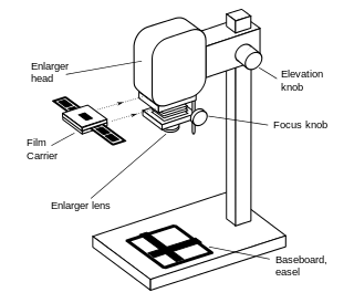
An enlarger is a specialized transparency projector used to produce photographic prints from film or glass negatives, or from transparencies.

A photogram is a photographic image made without a camera by placing objects directly onto the surface of a light-sensitive material such as photographic paper and then exposing it to light.
Masklesslithography (MPL) is a photomask-less photolithography-like technology used to project or focal-spot write the image pattern onto a chemical resist-coated substrate by means of UV radiation or electron beam.

A stepper or wafer stepper is a device used in the manufacture of integrated circuits (ICs). It is an essential part of the process of photolithography, which creates millions of microscopic circuit elements on the surface of silicon wafers out of which chips are made. It is similar in operation to a slide projector or a photographic enlarger. The ICs that are made form the heart of computer processors, memory chips, and many other electronic devices.
A via is an electrical connection between two or more metal layers, and are commonly used in printed circuit boards (PCB). Essentially a via is a small drilled hole that goes through two or more adjacent layers; the hole is plated with metal that forms an electrical connection through the insulating layers.

Computer-to-plate (CTP) is an imaging technology used in modern printing processes. In this technology, an image created in a desktop publishing (DTP) application is output directly to a printing plate.

Selective soldering is the process of selectively soldering components to printed circuit boards and molded modules that could be damaged by the heat of a reflow oven or wave soldering in a traditional surface-mount technology (SMT) or through-hole technology assembly processes. This usually follows an SMT oven reflow process; parts to be selectively soldered are usually surrounded by parts that have been previously soldered in a surface-mount reflow process, and the selective-solder process must be sufficiently precise to avoid damaging them.
Solder mask, solder stop mask or solder resist is a thin lacquer-like layer of polymer that is usually applied to the copper traces of a printed circuit board (PCB) for protection against oxidation and to prevent solder bridges from forming between closely spaced solder pads. A solder bridge is an unintended electrical connection between two conductors by means of a small blob of solder. PCBs use solder masks to prevent this from happening. Solder mask is not always used for hand soldered assemblies, but is essential for mass-produced boards that are soldered automatically using reflow or wave soldering techniques. Once applied, openings must be made in the solder mask wherever components are soldered, which is accomplished using photolithography. Solder mask is traditionally green, but is also available in many other colors.
Heinz Joseph Gerber was an American inventor and businessman. An Austrian-born Jewish Holocaust survivor who immigrated in 1940, he pioneered computer-automated manufacturing systems for an array of industries. Described as the "Thomas Edison of manufacturing", he was one of the first to recognize and develop the productivity-enhancing potential for computer automation in skill-intensive industrial sectors.
Stencil printing is the process of depositing solder paste on the printed wiring boards (PWBs) to establish electrical connections. It is immediately followed by the component placement stage. The equipment and materials used in this stage are a stencil, solder paste, and a printer.
A contact copier is a device used to copy an image by illuminating a film negative with the image in direct contact with a photosensitive surface. The more common processes are negative, where clear areas in the original produce an opaque or hardened photosensitive surface, but positive processes are available. The light source is usually an actinic bulb internal or external to the device
Reverse engineering of Printed circuit boards is the process of generating fabrication and design data for an existing circuit board, either closely or exactly replicating its functionality.
References
- ↑ Raymond H. Clark (6 December 2012). Handbook of Printed Circuit Manufacturing. Springer Science & Business Media. pp. 17–. ISBN 978-94-011-7012-3.
- ↑ Electronic Products. United Technical Publications. 1989.
- ↑ Electronic Packaging and Production. Cahners Pub. 1987.
- ↑ Carill Sharpe (1994). Kempe's Engineers Year-book. Morgan Bros.
- ↑ David J. Gerber (2015). The Inventor's Dilemma: The Remarkable Life of H. Joseph Gerber. Yale University Press. pp. 167–. ISBN 978-0-300-12350-0.
- 1 2 3 Chris Schroeder (1998). Printed Circuit Board Design Using AutoCAD. Newnes. ISBN 978-0-7506-9834-4.
- ↑ Jorge L.C. Sanz (1 December 1988). Advances in Machine Vision. Springer Science & Business Media. pp. 196–. ISBN 978-0-387-96822-3.
- 1 2 R. S. Khandpur (2005). Printed Circuit Boards: Design, Fabrication, Assembly and Testing. Tata McGraw-Hill Education. ISBN 978-0-07-058814-1.
- 1 2 Kraig Mitzner (28 May 2009). Complete PCB Design Using OrCAD Capture and PCB Editor. Newnes. ISBN 978-0-08-094354-1.