Piezoresistive effect

Last updated

The piezoresistive effect is a change in the electrical resistivity of a semiconductor or metal when mechanical strain is applied. In contrast to the piezoelectric effect, the piezoresistive effect causes a change only in electrical resistance, not in electric potential.

Contents

History

The change of electrical resistance in metal devices due to an applied mechanical load was first discovered in 1856 by Lord Kelvin. With single crystal silicon becoming the material of choice for the design of analog and digital circuits, the large piezoresistive effect in silicon and germanium was first discovered in 1954 (Smith 1954). [1]

Mechanism

In conducting and semi-conducting materials, changes in inter-atomic spacing resulting from strain affect the bandgaps, making it easier (or harder depending on the material and strain) for electrons to be raised into the conduction band. This results in a change in resistivity of the material. Within a certain range of strain this relationship is linear, so that the piezoresistive coefficient

where

ρ = Change in resistivity
ρ = Original resistivity
ε = Strain

are constant.

Piezoresistivity in metals

Usually the resistance change in metals is mostly due to the change of geometry resulting from applied mechanical stress. However, even though the piezoresistive effect is small in those cases it is often not negligible. In cases where it is, it can be calculated using the simple resistance equation derived from Ohm's law;

where

Conductor length [m]
A Cross-sectional area of the current flow [m2] [2] :p.207

Some metals display piezoresistivity that is much larger than the resistance change due to geometry. In platinum alloys, for instance, piezoresistivity is more than a factor of two larger, combining with the geometry effects to give a strain gauge sensitivity of up to more than three times as large than due to geometry effects alone. Pure nickel's piezoresistivity is -13 times larger, completely dwarfing and even reversing the sign of the geometry-induced resistance change.

Piezoresistive effect in bulk semiconductors

The piezoresistive effect of semiconductor materials can be several orders of magnitudes larger than the geometrical effect and is present in materials like germanium, polycrystalline silicon, amorphous silicon, silicon carbide, and single crystal silicon. Hence, semiconductor strain gauges with a very high coefficient of sensitivity can be built. For precision measurements they are more difficult to handle than metal strain gauges, because semiconductor strain gauges are generally sensitive to environmental conditions (especially temperature).

For silicon, gauge factors can be two orders of magnitudes larger than those observed in most metals (Smith 1954). The resistance of n-conducting silicon mainly changes due to a shift of the three different conducting valley pairs. The shifting causes a redistribution of the carriers between valleys with different mobilities. This results in varying mobilities dependent on the direction of current flow. A minor effect is due to the effective mass change related to changing shapes of the valleys. In p-conducting silicon the phenomena are more complex and also result in mass changes and hole transfer.

Giant piezoresistance in metal-silicon hybrid structures

A giant piezoresistive effect – where the piezoresistive coefficient exceeds the bulk value – was reported for a microfabricated silicon-aluminium hybrid structure. [3] The effect has been applied to silicon-based sensor technologies. [4]

Giant piezoresistive effect in silicon nanostructures

The longitudinal piezoresistive coefficient of top-down fabricated silicon nanowires was measured to be 60% larger than in bulk silicon. [5] [6] In 2006, giant piezoresistance [7] was reported in bottom-up fabricated silicon nanowires – a >30 increase in the longitudinal piezoresistive coefficient compared to bulk silicon was reported. The suggestion of a giant piezoresistance in nanostructures has since stimulated much effort into a physical understanding of the effect not only in silicon [8] [9] [10] [11] [12] [13] [14] but also in other functional materials. [15]

Piezoresistive silicon devices

The piezoresistive effect of semiconductors has been used for sensor devices employing all kinds of semiconductor materials such as germanium, polycrystalline silicon, amorphous silicon, and single crystal silicon. Since silicon is today the material of choice for integrated digital and analog circuits the use of piezoresistive silicon devices has been of great interest. It enables the easy integration of stress sensors with Bipolar and CMOS circuits.

This has enabled a wide range of products using the piezoresistive effect. Many commercial devices such as pressure sensors and acceleration sensors employ the piezoresistive effect in silicon. But due to its magnitude the piezoresistive effect in silicon has also attracted the attention of research and development for all other devices using single crystal silicon. Semiconductor Hall sensors, for example, were capable of achieving their current precision only after employing methods which eliminate signal contributions due to applied mechanical stress.

Piezoresistors

Piezoresistors are resistors made from a piezoresistive material and are usually used for measurement of mechanical stress. They are the simplest form of piezoresistive devices.

Fabrication

Piezoresistors can be fabricated using wide variety of piezoresistive materials. The simplest form of piezoresistive silicon sensors are diffused resistors. Piezoresistors consist of a simple two contact diffused n- or p-wells within a p- or n-substrate. As the typical square resistances of these devices are in the range of several hundred ohms, additional p+ or n+ plus diffusions are a potential method to facilitate ohmic contacts to the device.

Piezoresistor.jpg

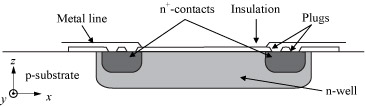
Schematic cross-section of the basic elements of a silicon n-well piezoresistor.

Physics of operation

For typical stress values in the MPa range the stress dependent voltage drop along the resistor Vr, can be considered to be linear. A piezoresistor aligned with the x-axis as shown in the figure may be described by

where , I, , , and denote the stress free resistance, the applied current, the transverse and longitudinal piezoresistive coefficients, and the three tensile stress components, respectively. The piezoresistive coefficients vary significantly with the sensor orientation with respect to the crystallographic axes and with the doping profile. Despite the fairly large stress sensitivity of simple resistors, they are preferably used in more complex configurations eliminating certain cross sensitivities and drawbacks. Piezoresistors have the disadvantage of being highly sensitive to temperature changes while featuring comparatively small relative stress dependent signal amplitude changes.

Other piezoresistive devices

In silicon the piezoresistive effect is used in piezoresistors, transducers, piezo-FETS, solid state accelerometers and bipolar transistors.

The electrically-conductive packaging material Velostat is used by hobbyists to make pressure sensors due to is piezoresistive properties and low cost.

See also

Related Research Articles

<span class="mw-page-title-main">Pressure measurement</span> Analysis of force applied by a fluid on a surface

Pressure measurement is the measurement of an applied force by a fluid on a surface. Pressure is typically measured in units of force per unit of surface area. Many techniques have been developed for the measurement of pressure and vacuum. Instruments used to measure and display pressure mechanically are called pressure gauges,vacuum gauges or compound gauges. The widely used Bourdon gauge is a mechanical device, which both measures and indicates and is probably the best known type of gauge.

Magnetoresistance is the tendency of a material to change the value of its electrical resistance in an externally-applied magnetic field. There are a variety of effects that can be called magnetoresistance. Some occur in bulk non-magnetic metals and semiconductors, such as geometrical magnetoresistance, Shubnikov–de Haas oscillations, or the common positive magnetoresistance in metals. Other effects occur in magnetic metals, such as negative magnetoresistance in ferromagnets or anisotropic magnetoresistance (AMR). Finally, in multicomponent or multilayer systems, giant magnetoresistance (GMR), tunnel magnetoresistance (TMR), colossal magnetoresistance (CMR), and extraordinary magnetoresistance (EMR) can be observed.

A nanowire is a nanostructure in the form of a wire with the diameter of the order of a nanometre. More generally, nanowires can be defined as structures that have a thickness or diameter constrained to tens of nanometers or less and an unconstrained length. At these scales, quantum mechanical effects are important—which coined the term "quantum wires".

<span class="mw-page-title-main">Electrical resistance and conductance</span> Opposition to the passage of an electric current

The electrical resistance of an object is a measure of its opposition to the flow of electric current. Its reciprocal quantity is electrical conductance, measuring the ease with which an electric current passes. Electrical resistance shares some conceptual parallels with mechanical friction. The SI unit of electrical resistance is the ohm, while electrical conductance is measured in siemens (S).

Electrical resistivity is a fundamental specific property of a material that measures its electrical resistance or how strongly it resists electric current. A low resistivity indicates a material that readily allows electric current. Resistivity is commonly represented by the Greek letter ρ (rho). The SI unit of electrical resistivity is the ohm-metre (Ω⋅m). For example, if a 1 m3 solid cube of material has sheet contacts on two opposite faces, and the resistance between these contacts is 1 Ω, then the resistivity of the material is 1 Ω⋅m.

<span class="mw-page-title-main">Strain gauge</span> Electronic component used to measure strain

A strain gauge is a device used to measure strain on an object. Invented by Edward E. Simmons and Arthur C. Ruge in 1938, the most common type of strain gauge consists of an insulating flexible backing which supports a metallic foil pattern. The gauge is attached to the object by a suitable adhesive, such as cyanoacrylate. As the object is deformed, the foil is deformed, causing its electrical resistance to change. This resistance change, usually measured using a Wheatstone bridge, is related to the strain by the quantity known as the gauge factor.

<span class="mw-page-title-main">Thermoelectric materials</span> Materials whose temperature variance leads to voltage change

Thermoelectric materials show the thermoelectric effect in a strong or convenient form.

<span class="mw-page-title-main">Nanoelectromechanical systems</span> Class of devices for nanoscale functionality

Nanoelectromechanical systems (NEMS) are a class of devices integrating electrical and mechanical functionality on the nanoscale. NEMS form the next logical miniaturization step from so-called microelectromechanical systems, or MEMS devices. NEMS typically integrate transistor-like nanoelectronics with mechanical actuators, pumps, or motors, and may thereby form physical, biological, and chemical sensors. The name derives from typical device dimensions in the nanometer range, leading to low mass, high mechanical resonance frequencies, potentially large quantum mechanical effects such as zero point motion, and a high surface-to-volume ratio useful for surface-based sensing mechanisms. Applications include accelerometers and sensors to detect chemical substances in the air.

<span class="mw-page-title-main">Giant magnetoresistance</span> Phenomenom involving the change of conductivity in metallic layers

Giant magnetoresistance (GMR) is a quantum mechanical magnetoresistance effect observed in multilayers composed of alternating ferromagnetic and non-magnetic conductive layers. The 2007 Nobel Prize in Physics was awarded to Albert Fert and Peter Grünberg for the discovery of GMR, which also sets the foundation for the study of spintronics.

Gauge factor (GF) or strain factor of a strain gauge is the ratio of relative change in electrical resistance R, to the mechanical strain ε. The gauge factor is defined as:

Nanoelectronics refers to the use of nanotechnology in electronic components. The term covers a diverse set of devices and materials, with the common characteristic that they are so small that inter-atomic interactions and quantum mechanical properties need to be studied extensively. Some of these candidates include: hybrid molecular/semiconductor electronics, one-dimensional nanotubes/nanowires or advanced molecular electronics.

Strain engineering refers to a general strategy employed in semiconductor manufacturing to enhance device performance. Performance benefits are achieved by modulating strain, as one example, in the transistor channel, which enhances electron mobility and thereby conductivity through the channel. Another example are semiconductor photocatalysts strain-engineered for more effective use of sunlight.

<span class="mw-page-title-main">Piezoelectric accelerometer</span> Type of accelerometer

A piezoelectric accelerometer is an accelerometer that employs the piezoelectric effect of certain materials to measure dynamic changes in mechanical variables.

<span class="mw-page-title-main">Force-sensing resistor</span> Material whose resistance changes when a force is applied

A force-sensing resistor is a material whose resistance changes when a force, pressure or mechanical stress is applied. They are also known as force-sensitive resistor and are sometimes referred to by the initialism FSR.

The inverse magnetostrictive effect, magnetoelastic effect or Villari effect, after its discoverer Emilio Villari, is the change of the magnetic susceptibility of a material when subjected to a mechanical stress.

In microscopy, scanning joule expansion microscopy (SJEM) is a form of scanning probe microscopy heavily based on atomic force microscopy (AFM) that maps the temperature distribution along a surface. Resolutions down to 10 nm have been achieved and 1 nm resolution is theoretically possible. Thermal measurements at the nanometer scale are of both academic and industrial interest, particularly in regards to nanomaterials and modern integrated circuits.

MEMS for in situ mechanical characterization refers to microelectromechanical systems (MEMS) used to measure the mechanical properties of nanoscale specimens such as nanowires, nanorods, whiskers, nanotubes and thin films. They distinguish themselves from other methods of nanomechanical testing because the sensing and actuation mechanisms are embedded and/or co-fabricated in the microsystem, providing—in the majority of cases—greater sensitivity and precision.

Piezotronics effect is using the piezoelectric potential (piezopotential) created in materials with piezoelectricity as a “gate” voltage to tune/control the charge carrier transport properties for fabricating new devices.

Band-gap engineering is the process of controlling or altering the band gap of a material. This is typically done to semiconductors by controlling the composition of alloys, constructing layered materials with alternating compositions, or by inducing strain either epitaxially or topologically. A band gap is the range in a solid where no electron state can exist. The band gap of insulators is much larger than in semiconductors. Conductors or metals have a much smaller or nonexistent band gap than semiconductors since the valence and conduction bands overlap. Controlling the band gap allows for the creation of desirable electrical properties.

In materials science, toughening refers to the process of making a material more resistant to the propagation of cracks. When a crack propagates, the associated irreversible work in different materials classes is different. Thus, the most effective toughening mechanisms differ among different materials classes. The crack tip plasticity is important in toughening of metals and long-chain polymers. Ceramics have limited crack tip plasticity and primarily rely on different toughening mechanisms.

References

  1. Barlian, A.A.; Park, W.-T.; Mallon, J.R.; Rastegar, A.J.; Pruitt, B.L. (March 2009). "Review: Semiconductor Piezoresistance for Microsystems". Proceedings of the IEEE. 97 (3): 513–552. doi:10.1109/jproc.2009.2013612. ISSN   0018-9219. PMC   2829857 . PMID   20198118.
  2. Liu, Chang (2006). "Piezoresistive Sensors" (PDF). Foundations of MEMS. Upper Saddle River, NG: Prentice Hall. ISBN   0131472860 . Retrieved March 3, 2013.
  3. Rowe, A. C. H.; Donoso-Barrera, A.; Renner, Ch.; Arscott, S. (April 8, 2008). "Giant Room-Temperature Piezoresistance in a Metal-Silicon Hybrid Structure". Physical Review Letters. 100 (14): 145501. arXiv: 0803.0655 . Bibcode:2008PhRvL.100n5501R. doi:10.1103/physrevlett.100.145501. ISSN   0031-9007. PMID   18518044. S2CID   42265969.
  4. Ngo, H.-D.; Tekin, T.; Vu, T.-C.; Fritz, M.; Kurniawan, W.; Mukhopadhyay, B.; Kolitsch, A.; Schiffer, M.; Lang, K.-D. (2011). MEMS sensor with giant piezoresistive effect using metall-semiconductor hybrid structure. 16th International Solid-State Sensors, Actuators and Microsystems Conference. IEEE. p. 1018-1021. doi:10.1109/transducers.2011.5969160.
  5. Toriyama, T.; Tanimoto, Y.; Sugiyama, S. (2002). "Single crystal silicon nano-wire piezoresistors for mechanical sensors". Journal of Microelectromechanical Systems. 11 (5). Institute of Electrical and Electronics Engineers (IEEE): 605–611. doi:10.1109/jmems.2002.802905. ISSN   1057-7157.
  6. Toriyama, T.; Sugiyama, S. (2003). "Single crystal silicon piezoresistive nano-wire bridge". Sensors and Actuators A: Physical. 108 (1–3). Elsevier BV: 244–249. doi:10.1016/s0924-4247(03)00269-3. ISSN   0924-4247.
  7. He, Rongrui; Yang, Peidong (2006). "Giant piezoresistance effect in silicon nanowires". Nature Nanotechnology. 1 (1). Springer Science and Business Media LLC: 42–46. Bibcode:2006NatNa...1...42H. doi:10.1038/nnano.2006.53. ISSN   1748-3387. PMID   18654140. S2CID   17694712.
  8. Allain, P. (November 8, 2012). Étude des propriétés électro-thermo-mécaniques de nanofils en silicium pour leur intégration dans les microsystèmes (Doctoral) (in French). Université Paris Sud . Retrieved October 31, 2021.
  9. Reck, K.; Richter, J.; Hansen, O.; Thomsen, E.V. (2008). Piezoresistive effect in top-down fabricated silicon nanowires. 2008 IEEE 21st International Conference on Micro Electro Mechanical Systems. IEEE. p. 7-17. doi:10.1109/memsys.2008.4443757. ISSN   1084-6999.
  10. Yang, Peidong (2008). "Chemistry and physics of silicon nanowire". Dalton Transactions (33). Royal Society of Chemistry (RSC): 4387–4391. doi:10.1039/b801440j. ISSN   1477-9226. PMID   18698439.
  11. Milne, J. S.; Rowe, A. C. H.; Arscott, S.; Renner, Ch. (November 23, 2010). "Giant Piezoresistance Effects in Silicon Nanowires and Microwires". Physical Review Letters. 105 (22): 226802. arXiv: 1010.1633 . Bibcode:2010PhRvL.105v6802M. doi:10.1103/physrevlett.105.226802. ISSN   0031-9007. PMID   21231411. S2CID   12201580.
  12. Koumela, A; Mercier, D; Dupré, C; Jourdan, G; Marcoux, C; Ollier, E; Purcell, S T; Duraffourg, L (September 2, 2011). "Piezoresistance of top-down suspended Si nanowires". Nanotechnology. 22 (39). IOP Publishing: 395701. Bibcode:2011Nanot..22M5701K. doi:10.1088/0957-4484/22/39/395701. ISSN   0957-4484. PMID   21891838. S2CID   24747354.
  13. Rowe, A.C.H. (March 28, 2014). "Piezoresistance in silicon and its nanostructures". Journal of Materials Research. 29 (6): 731–744. arXiv: 1309.6445 . Bibcode:2014JMatR..29..731R. doi:10.1557/jmr.2014.52. ISSN   0884-2914. S2CID   119238891.
  14. McClarty, M. M.; Jegenyes, N.; Gaudet, M.; Toccafondi, C.; Ossikovski, R.; Vaurette, F.; Arscott, S.; Rowe, A. C. H. (July 11, 2016). "Geometric and chemical components of the giant piezoresistance in silicon nanowires". Applied Physics Letters. 109 (2): 023102. arXiv: 1512.01396 . Bibcode:2016ApPhL.109b3102M. doi:10.1063/1.4955403. ISSN   0003-6951. S2CID   119189299.
  15. Ali, Utku Emre; Modi, Gaurav; Agarwal, Ritesh; Bhaskaran, Harish (March 18, 2022). "Real-time nanomechanical property modulation as a framework for tunable NEMS". Nature Communications. 13 (1): 1464. Bibcode:2022NatCo..13.1464A. doi:10.1038/s41467-022-29117-7. ISSN   2041-1723. PMC   8933423 . PMID   35304454.