Pole splitting

Last updated

Pole splitting is a phenomenon exploited in some forms of frequency compensation used in an electronic amplifier. When a capacitor is introduced between the input and output sides of the amplifier with the intention of moving the pole lowest in frequency (usually an input pole) to lower frequencies, pole splitting causes the pole next in frequency (usually an output pole) to move to a higher frequency. This pole movement increases the stability of the amplifier and improves its step response at the cost of decreased speed. [1] [2] [3] [4]

Contents

Example of pole splitting
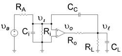
Figure 1: Operational amplifier with compensation capacitor CC between input and output; notice the amplifier has both input impedance Ri and output impedance Ro. Pole Splitting Example.png
Figure 1: Operational amplifier with compensation capacitor CC between input and output; notice the amplifier has both input impedance Ri and output impedance Ro.
Figure 2: Operational amplifier with compensation capacitor transformed using Miller's theorem to replace the compensation capacitor with a Miller capacitor at the input and a frequency-dependent current source at the output. Pole Splitting Example with Miller Transform.png
Figure 2: Operational amplifier with compensation capacitor transformed using Miller's theorem to replace the compensation capacitor with a Miller capacitor at the input and a frequency-dependent current source at the output.

This example shows that introduction of the capacitor referred to as CC in the amplifier of Figure 1 has two results: first it causes the lowest frequency pole of the amplifier to move still lower in frequency and second, it causes the higher pole to move higher in frequency. [5] The amplifier of Figure 1 has a low frequency pole due to the added input resistance Ri and capacitance Ci, with the time constant Ci ( RA || Ri ). This pole is moved down in frequency by the Miller effect. The amplifier is given a high frequency output pole by addition of the load resistance RL and capacitance CL, with the time constant CL ( Ro || RL ). The upward movement of the high-frequency pole occurs because the Miller-amplified compensation capacitor CC alters the frequency dependence of the output voltage divider.

The first objective, to show the lowest pole moves down in frequency, is established using the same approach as the Miller's theorem article. Following the procedure described in the article on Miller's theorem, the circuit of Figure 1 is transformed to that of Figure 2, which is electrically equivalent to Figure 1. Application of Kirchhoff's current law to the input side of Figure 2 determines the input voltage to the ideal op amp as a function of the applied signal voltage , namely,

which exhibits a roll-off with frequency beginning at f1 where

which introduces notation for the time constant of the lowest pole. This frequency is lower than the initial low frequency of the amplifier, which for CC = 0 F is .

Turning to the second objective, showing the higher pole moves still higher in frequency, it is necessary to look at the output side of the circuit, which contributes a second factor to the overall gain, and additional frequency dependence. The voltage is determined by the gain of the ideal op amp inside the amplifier as

Using this relation and applying Kirchhoff's current law to the output side of the circuit determines the load voltage as a function of the voltage at the input to the ideal op amp as:

This expression is combined with the gain factor found earlier for the input side of the circuit to obtain the overall gain as

This gain formula appears to show a simple two-pole response with two time constants. (It also exhibits a zero in the numerator but, assuming the amplifier gain Av is large, this zero is important only at frequencies too high to matter in this discussion, so the numerator can be approximated as unity.) However, although the amplifier does have a two-pole behavior, the two time-constants are more complicated than the above expression suggests because the Miller capacitance contains a buried frequency dependence that has no importance at low frequencies, but has considerable effect at high frequencies. That is, assuming the output R-C product, CL ( Ro || RL ), corresponds to a frequency well above the low frequency pole, the accurate form of the Miller capacitance must be used, rather than the Miller approximation. According to the article on Miller effect, the Miller capacitance is given by

(For a positive Miller capacitance, Av is negative.) Upon substitution of this result into the gain expression and collecting terms, the gain is rewritten as:

with Dω given by a quadratic in ω, namely:

Every quadratic has two factors, and this expression looks simpler if it is rewritten as

where and are combinations of the capacitances and resistances in the formula for Dω. [6] They correspond to the time constants of the two poles of the amplifier. One or the other time constant is the longest; suppose is the longest time constant, corresponding to the lowest pole, and suppose >> . (Good step response requires >> . See Selection of CC below.)

At low frequencies near the lowest pole of this amplifier, ordinarily the linear term in ω is more important than the quadratic term, so the low frequency behavior of Dω is:

where now CM is redefined using the Miller approximation as

which is simply the previous Miller capacitance evaluated at low frequencies. On this basis is determined, provided >> . Because CM is large, the time constant is much larger than its original value of Ci ( RA || Ri ). [7]

At high frequencies the quadratic term becomes important. Assuming the above result for is valid, the second time constant, the position of the high frequency pole, is found from the quadratic term in Dω as

Substituting in this expression the quadratic coefficient corresponding to the product along with the estimate for , an estimate for the position of the second pole is found:

and because CM is large, it seems is reduced in size from its original value CL ( Ro || RL ); that is, the higher pole has moved still higher in frequency because of CC. [8]

In short, introduction of capacitor CC moved the low pole lower and the high pole higher, so the term pole splitting seems a good description.

Selection of CC

Figure 3: Idealized Bode plot for a two pole amplifier design. Gain drops from first pole at f1 at 20 dB / decade down to second pole at f2 where the slope increases to 40 dB / decade. Two-pole Bode magnitude plot.png
Figure 3: Idealized Bode plot for a two pole amplifier design. Gain drops from first pole at f1 at 20 dB / decade down to second pole at f2 where the slope increases to 40 dB / decade.

What value is a good choice for CC? For general purpose use, traditional design (often called dominant-pole or single-pole compensation) requires the amplifier gain to drop at 20 dB/decade from the corner frequency down to 0 dB gain, or even lower. [9] [10] With this design the amplifier is stable and has near-optimal step response even as a unity gain voltage buffer. A more aggressive technique is two-pole compensation. [11] [12]

The way to position f2 to obtain the design is shown in Figure 3. At the lowest pole f1, the Bode gain plot breaks slope to fall at 20 dB/decade. The aim is to maintain the 20 dB/decade slope all the way down to zero dB, and taking the ratio of the desired drop in gain (in dB) of 20 log10Av to the required change in frequency (on a log frequency scale [13] ) of ( log10f2  log10f1 ) = log10 ( f2 / f1 ) the slope of the segment between f1 and f2 is:

Slope per decade of frequency

which is 20 dB/decade provided f2 = Av f1 . If f2 is not this large, the second break in the Bode plot that occurs at the second pole interrupts the plot before the gain drops to 0 dB with consequent lower stability and degraded step response.

Figure 3 shows that to obtain the correct gain dependence on frequency, the second pole is at least a factor Av higher in frequency than the first pole. The gain is reduced a bit by the voltage dividers at the input and output of the amplifier, so with corrections to Av for the voltage dividers at input and output the pole-ratio condition for good step response becomes:

Figure 4: Miller capacitance at low frequencies CM (top) and compensation capacitor CC (bottom) as a function of gain using Excel. Capacitance units are pF. Compensation capacitance.png
Figure 4: Miller capacitance at low frequencies CM (top) and compensation capacitor CC (bottom) as a function of gain using Excel. Capacitance units are pF.

Using the approximations for the time constants developed above,

or

which provides a quadratic equation to determine an appropriate value for CC. Figure 4 shows an example using this equation. At low values of gain this example amplifier satisfies the pole-ratio condition without compensation (that is, in Figure 4 the compensation capacitor CC is small at low gain), but as gain increases, a compensation capacitance rapidly becomes necessary (that is, in Figure 4 the compensation capacitor CC increases rapidly with gain) because the necessary pole ratio increases with gain. For still larger gain, the necessary CC drops with increasing gain because the Miller amplification of CC, which increases with gain (see the Miller equation ), allows a smaller value for CC.

To provide more safety margin for design uncertainties, often Av is increased to two or three times Av on the right side of this equation. [14] See Sansen [4] or Huijsing [10] and article on step response.

Slew rate

The above is a small-signal analysis. However, when large signals are used, the need to charge and discharge the compensation capacitor adversely affects the amplifier slew rate; in particular, the response to an input ramp signal is limited by the need to charge CC.

See also

References and notes

  1. That is, the rise time is selected to be the fastest possible consistent with low overshoot and ringing.
  2. C. Toumazu, Moschytz GS & Gilbert B (Editors) (2007). Trade-offs in analog circuit design: the designer's companion. New York/Berlin/Dordrecht: Springer. pp. 272–275. ISBN   978-1-4020-7037-2.{{cite book}}: |author= has generic name (help)
  3. Marc T. Thompson (2006). Intuitive analog circuit design: a problem-solving approach using design case studies. Amsterdam: Elsevier Newnes. p. 200. ISBN   0-7506-7786-4.
  4. 1 2 Willy M. C. Sansen (2006). Analog design essentials. New York; Berlin: Springer. pp. §097, p. 266 et seq. ISBN   0-387-25746-2.
  5. Although this example appears very specific, the associated mathematical analysis is very much used in circuit design.
  6. The sum of the time constants is the coefficient of the term linear in jω and the product of the time constants is the coefficient of the quadratic term in (jω)2.
  7. The expression for differs a little from ( CM+Ci ) ( RA || Ri ) as found initially for f1, but the difference is minor assuming the load capacitance is not so large that it controls the low frequency response instead of the Miller capacitance.
  8. As an aside, the higher the high-frequency pole is made in frequency, the more likely it becomes for a real amplifier that other poles (not considered in this analysis) play a part.
  9. A.S. Sedra and K.C. Smith (2004). Microelectronic circuits (Fifth ed.). New York: Oxford University Press. pp. 849 and Example 8.6, p. 853. ISBN   0-19-514251-9.
  10. 1 2 Huijsing, Johan H. (2001). Operational amplifiers: theory and design. Boston, MA: Kluwer Academic. pp. §6.2, pp.205–206 and Figure 6.2.1. ISBN   0-7923-7284-0.
  11. Feucht, Dennis: Two-pole compensation
  12. Self, Douglas (2006). Audio power amplifier design handbook. Oxford: Newnes. pp. 191–193. ISBN   0-7506-8072-5.
  13. That is, the frequency is plotted in powers of ten, as 1, 10, 102etc.
  14. A factor of two results in the maximally flat or Butterworth design for a two-pole amplifier. However, real amplifiers have more than two poles, and a factor greater than two often is necessary.

Related Research Articles

In classical mechanics, a harmonic oscillator is a system that, when displaced from its equilibrium position, experiences a restoring force F proportional to the displacement x:

Bode plot

In electrical engineering and control theory, a Bode plot is a graph of the frequency response of a system. It is usually a combination of a Bode magnitude plot, expressing the magnitude of the frequency response, and a Bode phase plot, expressing the phase shift.

A resistor–capacitor circuit, or RC filter or RC network, is an electric circuit composed of resistors and capacitors. It may be driven by a voltage or current source and these will produce different responses. A first order RC circuit is composed of one resistor and one capacitor and is the simplest type of RC circuit.

Voltage divider Linear circuit that produces an output voltage that is a fraction of its input voltage

In electronics, a voltage divider is a passive linear circuit that produces an output voltage (Vout) that is a fraction of its input voltage (Vin). Voltage division is the result of distributing the input voltage among the components of the divider. A simple example of a voltage divider is two resistors connected in series, with the input voltage applied across the resistor pair and the output voltage emerging from the connection between them.

Step response

The step response of a system in a given initial state consists of the time evolution of its outputs when its control inputs are Heaviside step functions. In electronic engineering and control theory, step response is the time behaviour of the outputs of a general system when its inputs change from zero to one in a very short time. The concept can be extended to the abstract mathematical notion of a dynamical system using an evolution parameter.

Butterworth filter Type of signal processing filter

The Butterworth filter is a type of signal processing filter designed to have a frequency response that is as flat as possible in the passband. It is also referred to as a maximally flat magnitude filter. It was first described in 1930 by the British engineer and physicist Stephen Butterworth in his paper entitled "On the Theory of Filter Amplifiers".

In electronics, when describing a voltage or current step function, rise time is the time taken by a signal to change from a specified low value to a specified high value. These values may be expressed as ratios or, equivalently, as percentages with respect to a given reference value. In analog electronics and digital electronics, these percentages are commonly the 10% and 90% of the output step height: however, other values are commonly used. For applications in control theory, according to Levine, rise time is defined as "the time required for the response to rise from x% to y% of its final value", with 0% to 100% rise time common for underdamped second order systems, 5% to 95% for critically damped and 10% to 90% for overdamped ones. According to Orwiler, the term "rise time" applies to either positive or negative step response, even if a displayed negative excursion is popularly termed fall time.

Linear time-invariant system Mathematical model

In system analysis, among other fields of study, a linear time-invariant system is a system that produces an output signal from any input signal subject to the constraints of linearity and time-invariance; these terms are briefly defined below. These properties apply to many important physical systems, in which case the response y(t) of the system to an arbitrary input x(t) can be found directly using convolution: y(t) = x(t) ∗ h(t) where h(t) is called the system's impulse response and ∗ represents convolution. What's more, there are systematic methods for solving any such system, whereas systems not meeting both properties are generally more difficult to solve analytically. A good example of an LTI system is any electrical circuit consisting of resistors, capacitors, inductors and linear amplifiers.

Common source Electronic amplifier circuit type

In electronics, a common-source amplifier is one of three basic single-stage field-effect transistor (FET) amplifier topologies, typically used as a voltage or transconductance amplifier. The easiest way to tell if a FET is common source, common drain, or common gate is to examine where the signal enters and leaves. The remaining terminal is what is known as "common". In this example, the signal enters the gate, and exits the drain. The only terminal remaining is the source. This is a common-source FET circuit. The analogous bipolar junction transistor circuit may be viewed as a transconductance amplifier or as a voltage amplifier.. As a transconductance amplifier, the input voltage is seen as modulating the current going to the load. As a voltage amplifier, input voltage modulates the current flowing through the FET, changing the voltage across the output resistance according to Ohm's law. However, the FET device's output resistance typically is not high enough for a reasonable transconductance amplifier, nor low enough for a decent voltage amplifier. Another major drawback is the amplifier's limited high-frequency response. Therefore, in practice the output often is routed through either a voltage follower, or a current follower, to obtain more favorable output and frequency characteristics. The CS–CG combination is called a cascode amplifier.

A resistor–inductor circuit, or RL filter or RL network, is an electric circuit composed of resistors and inductors driven by a voltage or current source. A first-order RL circuit is composed of one resistor and one inductor, either in series driven by a voltage source or in parallel driven by a current source. It is one of the simplest analogue infinite impulse response electronic filters.

Gain–bandwidth product

The gain–bandwidth product for an amplifier is the product of the amplifier's bandwidth and the gain at which the bandwidth is measured.

In electronics, the Miller effect accounts for the increase in the equivalent input capacitance of an inverting voltage amplifier due to amplification of the effect of capacitance between the input and output terminals. The virtually increased input capacitance due to the Miller effect is given by

Parasitic capacitance is an unavoidable and usually unwanted capacitance that exists between the parts of an electronic component or circuit simply because of their proximity to each other. When two electrical conductors at different voltages are close together, the electric field between them causes electric charge to be stored on them; this effect is capacitance.

Resonance fluorescence is the process in which a two-level atom system interacts with the quantum electromagnetic field if the field is driven at a frequency near to the natural frequency of the atom.

The open-circuit time constant (OCT) method is an approximate analysis technique used in electronic circuit design to determine the corner frequency of complex circuits. It is a special case of zero-value time constant (ZVT) method technique when reactive elements consist of only capacitors. The zero-value time (ZVT) constant method itself is a special case of the general Time- and Transfer Constant (TTC) analysis that allows full evaluation of the zeros and poles of any lumped LTI systems of with both inductors and capacitors as reactive elements using time constants and transfer constants. The OCT method provides a quick evaluation, and identifies the largest contributions to time constants as a guide to the circuit improvements.

In physics and engineering, the time constant, usually denoted by the Greek letter τ (tau), is the parameter characterizing the response to a step input of a first-order, linear time-invariant (LTI) system. The time constant is the main characteristic unit of a first-order LTI system.

An LC circuit can be quantized using the same methods as for the quantum harmonic oscillator. An LC circuit is a variety of resonant circuit, and consists of an inductor, represented by the letter L, and a capacitor, represented by the letter C. When connected together, an electric current can alternate between them at the circuit's resonant frequency:

RLC circuit Resistor Inductor Capacitor Circuit

An RLC circuit is an electrical circuit consisting of a resistor (R), an inductor (L), and a capacitor (C), connected in series or in parallel. The name of the circuit is derived from the letters that are used to denote the constituent components of this circuit, where the sequence of the components may vary from RLC.

In thermal quantum field theory, the Matsubara frequency summation is the summation over discrete imaginary frequencies. It takes the following form

Staggered tuning is a technique used in the design of multi-stage tuned amplifiers whereby each stage is tuned to a slightly different frequency. In comparison to synchronous tuning it produces a wider bandwidth at the expense of reduced gain. It also produces a sharper transition from the passband to the stopband. Both staggered tuning and synchronous tuning circuits are easier to tune and manufacture than many other filter types.