Related Research Articles

In mechanics and physics, shock is a sudden acceleration caused, for example, by impact, drop, kick, earthquake, or explosion. Shock is a transient physical excitation.
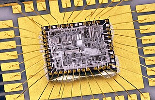
Wire bonding is a method of making interconnections between an integrated circuit (IC) or other semiconductor device and its packaging during semiconductor device fabrication. Wire bonding can also be used to connect an IC to other electronics or to connect from one printed circuit board (PCB) to another, although these are less common. Wire bonding is generally considered the most cost-effective and flexible interconnect technology and is used to assemble the vast majority of semiconductor packages. Wire bonding can be used at frequencies above 100 GHz.

Medium-density fibreboard (MDF) is an engineered wood product made by breaking down hardwood or softwood residuals into wood fibre, often in a defibrator, combining it with wax and a resin binder, and forming it into panels by applying high temperature and pressure. MDF is generally denser than plywood. It is made up of separated fibre but can be used as a building material similar in application to plywood. It is stronger and denser than particle board.

The flash point of a material is the "lowest liquid temperature at which, under certain standardized conditions, a liquid gives off vapours in a quantity such as to be capable of forming an ignitable vapour/air mixture".

Flip chip, also known as controlled collapse chip connection or its abbreviation, C4, is a method for interconnecting dies such as semiconductor devices, IC chips, integrated passive devices and microelectromechanical systems (MEMS), to external circuitry with solder bumps that have been deposited onto the chip pads. The technique was developed by General Electric's Light Military Electronics Department, Utica, New York. The solder bumps are deposited on the chip pads on the top side of the wafer during the final wafer processing step. In order to mount the chip to external circuitry, it is flipped over so that its top side faces down, and aligned so that its pads align with matching pads on the external circuit, and then the solder is reflowed to complete the interconnect. This is in contrast to wire bonding, in which the chip is mounted upright and fine wires are welded onto the chip pads and lead frame contacts to interconnect the chip pads to external circuitry.

Integrated circuit packaging is the final stage of semiconductor device fabrication, in which the die is encapsulated in a supporting case that prevents physical damage and corrosion. The case, known as a "package", supports the electrical contacts which connect the device to a circuit board.

Magnetic particle inspection (MPI) is a nondestructive testing process where a magnetic field is used for detecting surface, and shallow subsurface, discontinuities in ferromagnetic materials. Examples of ferromagnetic materials include iron, nickel, cobalt, and some of their alloys. The process puts a magnetic field into the part. The piece can be magnetized by direct or indirect magnetization. Direct magnetization occurs when the electric current is passed through the test object and a magnetic field is formed in the material. Indirect magnetization occurs when no electric current is passed through the test object, but a magnetic field is applied from an outside source. The magnetic lines of force are perpendicular to the direction of the electric current, which may be either alternating current (AC) or some form of direct current (DC).
Electric resistance welding (ERW) is a welding process in which metal parts in contact are permanently joined by heating them with an electric current, melting the metal at the joint. Electric resistance welding is widely used, for example, in manufacture of steel pipe and in assembly of bodies for automobiles. The electric current can be supplied to electrodes that also apply clamping pressure, or may be induced by an external magnetic field. The electric resistance welding process can be further classified by the geometry of the weld and the method of applying pressure to the joint: spot welding, seam welding, flash welding, projection welding, for example. Some factors influencing heat or welding temperatures are the proportions of the workpieces, the metal coating or the lack of coating, the electrode materials, electrode geometry, electrode pressing force, electric current and length of welding time. Small pools of molten metal are formed at the point of most electrical resistance as an electric current is passed through the metal. In general, resistance welding methods are efficient and cause little pollution, but their applications are limited to relatively thin materials.
The solderability of a substrate is a measure of the ease with which a soldered joint can be made to that material. Good solderability requires wetting of the substrate by the solder.

A heat sealer is a machine used to seal products, packaging, and other thermoplastic materials using heat. This can be with uniform thermoplastic monolayers or with materials having several layers, at least one being thermoplastic. Heat sealing can join two similar materials together or can join dissimilar materials, one of which has a thermoplastic layer.
Design for testing or design for testability (DFT) consists of IC design techniques that add testability features to a hardware product design. The added features make it easier to develop and apply manufacturing tests to the designed hardware. The purpose of manufacturing tests is to validate that the product hardware contains no manufacturing defects that could adversely affect the product's correct functioning.

Pressure-sensitive adhesive is a type of nonreactive adhesive which forms a bond when pressure is applied to bond the adhesive with a surface. No solvent, water, or heat is needed to activate the adhesive. It is used in pressure-sensitive tapes, labels, glue dots, stickers, sticky note pads, automobile trim, and a wide variety of other products.

A universal testing machine (UTM), also known as a universal tester, universal tensile machine, materials testing machine, materials test frame, is used to test the tensile strength (pulling) and compressive strength (pushing), flexural strength, bending, shear, hardness, and torsion testing, providing valuable data for designing and ensuring the quality of materials. An earlier name for a tensile testing machine is a tensometer. The "universal" part of the name reflects that it can perform many standard tests application on materials, components, and structures.
The MIL-STD-883 standard establishes uniform methods, controls, and procedures for testing microelectronic devices suitable for use within military and aerospace electronic systems including basic environmental tests to determine resistance to deleterious effects of natural elements and conditions surrounding military and space operations; mechanical and electrical tests; workmanship and training procedures; and such other controls and constraints as have been deemed necessary to ensure a uniform level of quality and reliability suitable to the intended applications of those devices. For this standard, the term "devices" includes monolithic, multichip, film and hybrid microcircuits, microcircuit arrays, and the elements from which the circuits and arrays are formed. This standard is intended to apply only to microelectronic devices.
Reliability of a semiconductor device is the ability of the device to perform its intended function during the life of the device in the field.

Package testing or packaging testing involves the measurement of a characteristic or property involved with packaging. This includes packaging materials, packaging components, primary packages, shipping containers, and unit loads, as well as the associated processes.
The wafer bond characterization is based on different methods and tests. Considered a high importance of the wafer are the successful bonded wafers without flaws. Those flaws can be caused by void formation in the interface due to unevenness or impurities. The bond connection is characterized for wafer bond development or quality assessment of fabricated wafers and sensors.
A bond tester is a scientific instrument used to measure the mechanical strength of bonds, evaluate bond strength distributions or determine compliance with specified bond strength requirements of the applicable acquisition document.
Polytetrafluoroethylene (PTFE), better known by its trade name Teflon, has many desirable properties which make it an attractive material for numerous industries. It has good chemical resistance, a low dielectric constant, low dielectric loss, and a low coefficient of friction, making it ideal for reactor linings, circuit boards, and kitchen utensils, to name a few applications. However, its nonstick properties make it challenging to bond to other materials or to itself.

Package handles, or carriers, are used to help people use packaging. They are designed to simplify and to improve the ergonomics of lifting and carrying packages. Handles on consumer packages add convenience and help facilitate use and pouring. The effect of handles on package material costs and the packaging line efficiencies are also critical. A handle can be defined as “an accessory attached to a container or part for the purpose of holding or carrying.” Sometimes a handle can be used to hang a package for dispensing or use.
References
- ↑ "MIL-STD-883 2011.9 bond strength (bond pull test)".
- ↑ "MIL-STD-883 method 2031.1 Flip-chip pull-off test". Archived from the original on 2019-10-08.
- ↑ BS 1881-201: 1986
- ↑ "ASTM Standard for Pull-Off Test". ASTM.
| | This standards- or measurement-related article is a stub. You can help Wikipedia by expanding it. |