The quantum Hall effect is a quantized version of the Hall effect which is observed in two-dimensional electron systems subjected to low temperatures and strong magnetic fields, in which the Hall resistance Rxy exhibits steps that take on the quantized values
A nanowire is a nanostructure in the form of a wire with the diameter of the order of a nanometre. More generally, nanowires can be defined as structures that have a thickness or diameter constrained to tens of nanometers or less and an unconstrained length. At these scales, quantum mechanical effects are important—which coined the term "quantum wires".
Electrical resistivity is a fundamental specific property of a material that measures its electrical resistance or how strongly it resists electric current. A low resistivity indicates a material that readily allows electric current. Resistivity is commonly represented by the Greek letter ρ (rho). The SI unit of electrical resistivity is the ohm-metre (Ω⋅m). For example, if a 1 m3 solid cube of material has sheet contacts on two opposite faces, and the resistance between these contacts is 1 Ω, then the resistivity of the material is 1 Ω⋅m.

In physics and electrical engineering, a conductor is an object or type of material that allows the flow of charge in one or more directions. Materials made of metal are common electrical conductors. The flow of negatively charged electrons generates electric current, positively charged holes, and positive or negative ions in some cases.
In mesoscopic physics, a Coulomb blockade (CB), named after Charles-Augustin de Coulomb's electrical force, is the decrease in electrical conductance at small bias voltages of a small electronic device comprising at least one low-capacitance tunnel junction. Because of the CB, the conductance of a device may not be constant at low bias voltages, but disappear for biases under a certain threshold, i.e. no current flows.
In mesoscopic physics, ballistic conduction is the unimpeded flow of charge carriers, or energy-carrying particles, over relatively long distances in a material. In general, the resistivity of a material exists because an electron, while moving inside a medium, is scattered by impurities, defects, thermal fluctuations of ions in a crystalline solid, or, generally, by any freely-moving atom/molecule composing a gas or liquid. Without scattering, electrons simply obey Newton's second law of motion at non-relativistic speeds.
The conductance quantum, denoted by the symbol G0, is the quantized unit of electrical conductance. It is defined by the elementary charge e and Planck constant h as:
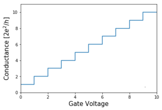
A quantum point contact (QPC) is a narrow constriction between two wide electrically conducting regions, of a width comparable to the electronic wavelength.

Mesoscopic physics is a subdiscipline of condensed matter physics that deals with materials of an intermediate size. These materials range in size between the nanoscale for a quantity of atoms and of materials measuring micrometres. The lower limit can also be defined as being the size of individual atoms. At the microscopic scale are bulk materials. Both mesoscopic and macroscopic objects contain many atoms. Whereas average properties derived from constituent materials describe macroscopic objects, as they usually obey the laws of classical mechanics, a mesoscopic object, by contrast, is affected by thermal fluctuations around the average, and its electronic behavior may require modeling at the level of quantum mechanics.
Universal conductance fluctuations(UCF) in mesoscopic physics is a phenomenon encountered in electrical transport experiments in mesoscopic species. The measured electrical conductance will vary from sample to sample, mainly due to inhomogeneous scattering sites. Fluctuations originate from coherence effects for electronic wavefunctions and thus the phase-coherence length needs be larger than the momentum relaxation length . UCF is more profound when electrical transport is in weak localization regime. where , is the number of conduction channels and is the momentum relaxation due to phonon scattering events length or mean free path. For weakly localized samples fluctuation in conductance is equal to fundamental conductance regardless of the number of channels.
Organic photovoltaic devices (OPVs) are fabricated from thin films of organic semiconductors, such as polymers and small-molecule compounds, and are typically on the order of 100 nm thick. Because polymer based OPVs can be made using a coating process such as spin coating or inkjet printing, they are an attractive option for inexpensively covering large areas as well as flexible plastic surfaces. A promising low cost alternative to conventional solar cells made of crystalline silicon, there is a large amount of research being dedicated throughout industry and academia towards developing OPVs and increasing their power conversion efficiency.
The optical properties of carbon nanotubes are highly relevant for materials science. The way those materials interact with electromagnetic radiation is unique in many respects, as evidenced by their peculiar absorption, photoluminescence (fluorescence), and Raman spectra.
A carbon nanotube quantum dot is a small region of a carbon nanotube in which electrons are confined.

Transparent conducting films (TCFs) are thin films of optically transparent and electrically conductive material. They are an important component in a number of electronic devices including liquid-crystal displays, OLEDs, touchscreens and photovoltaics. While indium tin oxide (ITO) is the most widely used, alternatives include wider-spectrum transparent conductive oxides (TCOs), conductive polymers, metal grids and random metallic networks, carbon nanotubes (CNT), graphene, nanowire meshes and ultra thin metal films.

A force-sensing resistor is a material whose resistance changes when a force, pressure or mechanical stress is applied. They are also known as force-sensitive resistor and are sometimes referred to by the initialism FSR.
The transport of heat in solids involves both electrons and vibrations of the atoms (phonons). When the solid is perfectly ordered over hundreds of thousands of atoms, this transport obeys established physics. However, when the size of the ordered regions decreases new physics can arise, thermal transport in nanostructures. In some cases heat transport is more effective, in others it is not.
A carbon nanotube field-effect transistor (CNTFET) is a field-effect transistor that utilizes a single carbon nanotube (CNT) or an array of carbon nanotubes as the channel material, instead of bulk silicon, as in the traditional MOSFET structure. There have been major developments since CNTFETs were first demonstrated in 1998.
Single-walled carbon nanotubes in the fields of quantum mechanics and nanoelectronics, have the ability to conduct electricity. This conduction can be ballistic, diffusive, or based on scattering. When ballistic in nature conductance can be treated as if the electrons experience no scattering.
In nanotechnology, carbon nanotube interconnects refer to the proposed use of carbon nanotubes in the interconnects between the elements of an integrated circuit. Carbon nanotubes (CNTs) can be thought of as single atomic layer graphite sheets rolled up to form seamless cylinders. Depending on the direction on which they are rolled, CNTs can be semiconducting or metallic. Metallic carbon nanotubes have been identified as a possible interconnect material for the future technology generations and to replace copper interconnects. Electron transport can go over long nanotube lengths, 1 μm, enabling CNTs to carry very high currents (i.e. up to a current density of 109 A∙cm−2) with essentially no heating due to nearly one dimensional electronic structure. Despite the current saturation in CNTs at high fields, the mitigation of such effects is possible due to encapsulated nanowires.
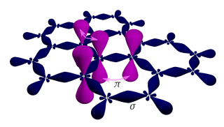
Graphene is a semimetal whose conduction and valence bands meet at the Dirac points, which are six locations in momentum space, the vertices of its hexagonal Brillouin zone, divided into two non-equivalent sets of three points. The two sets are labeled K and K'. The sets give graphene a valley degeneracy of gv = 2. By contrast, for traditional semiconductors the primary point of interest is generally Γ, where momentum is zero. Four electronic properties separate it from other condensed matter systems.


