SU-8 photoresist

Last updated
SU-8 molecule SU-8 photoresist.png
SU-8 molecule

SU-8 is a commonly used epoxy-based negative photoresist. Negative refers to a photoresist whereby the parts exposed to UV become cross-linked, while the remainder of the film remains soluble and can be washed away during development.

Contents

As shown in the structural diagram, SU-8 derives its name from the presence of 8 epoxy groups. This is a statistical average per moiety. It is these epoxies that cross-link to give the final structure.

It can be made into a viscous polymer that can be spun or spread over a thickness ranging from below 1 micrometer up to above 300 micrometers, or Thick Film Dry Sheets (TFDS) for lamination up to above 1 millimetre thick. Up to 500 µm, the resist can be processed with standard contact lithography. [1] Above 500 µm, absorption leads to increasing sidewall undercuts and poor curing at the substrate interface. It can be used to pattern high aspect ratio structures. An aspect ratio of (> 20) has been achieved with the solution formulation [2] and (> 40) has been demonstrated from the dry resist. [3] Its maximum absorption is for ultraviolet light with a wavelength of the i-line: 365 nm (it is not practical to expose SU-8 with g-line ultraviolet light). When exposed, SU-8's long molecular chains cross-link, causing the polymerisation of the material. SU-8 series photoresists use gamma-butyrolactone or cyclopentanone as the primary solvent.

SU-8 was originally developed as a photoresist for the microelectronics industry, to provide a high-resolution mask for fabrication of semiconductor devices.

It is now mainly used in the fabrication of microfluidics (mainly via soft lithography, but also with other imprinting techniques such as nanoimprint lithography [4] ) and microelectromechanical systems parts. It is also one of the most biocompatible materials known [5] and is often used in bio-MEMS for life science applications. [6]

Composition and processing

SU-8 is composed of Bisphenol A Novolac epoxy that is dissolved in an organic solvent (gamma-butyrolactone GBL or cyclopentanone, depending on the formulation) and up to 10 wt% of mixed Triarylsulfonium/hexafluoroantimonate salt as the photoacid generator. [7]

SU-8 absorbs light in the UV region, allowing fabrication of relatively thick (hundreds of micrometers) structures with nearly vertical side walls. The fact that a single photon can trigger multiple polymerizations makes the SU-8 a chemically amplified resist which is polymerized by photoacid generation. [8] The light irradiated on the resist interacts with the salt in the solution, creating hexafluoroantimonic acid that then protonates the epoxides groups in the resin monomers. The monomer are thus activated but the polymerization will not proceed significantly until the temperature is raised as part of the post-expose bake. It is at this stage that the epoxy groups in the resin cross-link to form the cured structure. When fully cured, the high crosslinking degree gives to the resist its excellent mechanical properties. [9]

The processing of SU-8 is similar to other negative resists with particular attention on the control of the temperature in the baking steps. The baking times depend on the SU-8 layer thickness; the thicker the layer, the longer the baking time. The temperature is controlled during the baking in order to reduce stress formation in the thick layer (leading to cracks) as the solvent evaporates.

The soft bake is the most important of the bake steps for stress formation. It is performed after spin coating. Its function is to remove the solvent from the resist and make the layer solid. Typically at least 5% of the solvent remains in the layer after the soft bake, however the thicker the coating, the harder it becomes to remove the solvent, as evaporating solvent through thick layers becomes increasingly difficult with coating thickness. The bake is performed on a programmable hot plate to reduce the skinning effect of solvent depletion at the surface creating a dense layer which makes the remainder of the solvent more difficult to remove. In order to reduce stress, the bake procedure is generally a two-step process made up of holding at 65 °C before ramping to 95 °C and holding again for a time dependent on the layer thickness. The temperature is then lowered slowly to room temperature.

When dry films are used, the photoresist is laminated rather than spin-coated. As this formulation is essentially solventless (less than 1% solvent remaining), it does not require a soft bake step and does not suffer stress or skinning. For enhanced adhesion, a post lamination bake can be added. This step is carried out in a similar way to the solution based resist - i.e. holding at 65 °C then 95 °C, the time dependent on film thickness.

After this stage the SU-8 layer can now be exposed. Typically this is through a photomask with an inverse pattern, as the resist is negative. The exposure time is a function of exposure dose and film thickness. After exposure the SU-8 needs to be baked again to complete the polymerization. This baking step is not as critical as the prebake but the rising of the temperature (again to 95 °C) needs to be slow and controlled. At this point the resist is ready to be developed.

The main developer for SU-8 is 1-methoxy-2-propanol acetate. [10] Development time is primarily a function of SU-8 thickness.

After exposing and developing, its highly cross-linked structure gives it high stability to chemicals and radiation damage - hence the name "resist". Cured cross-linked SU-8 shows very low levels of outgassing in a vacuum. [11] [12] However it is very difficult to remove, and tends to outgas in an unexposed state. [13]

Newer formulations

SU-8 2000 series resists use cyclopentanone for the primary solvent and can be used to create films between 0.5 and 100 µm in thickness. This formulation may offer improved adhesion on some substrates versus the original formulation. [14]

SU-8 3000 series resists also use cyclopentanone for the primary solvent and are designed to be spun into thicker films ranging from 2 to 75 µm in a single coat. [14]

SU-8 GLM2060 series of low-stress photoresist consist of epoxy GBL and silica formulation CTE 14. [15]

SU-8 GCM3060 Series of GERSTELTEC conductive SU8 with nanoparticles of silver. [15]

SU-8 GMC10xx Series of GERSTELTEC colored SU8 Red, Bleau, Green, black and others. [15]

SU-8 GMJB10XX Series of GERSTELTEC low viscosities epoxy for inkjet applications. [15]

SU8 GM10XX Series of Classic GERSTELTEC epoxy. [16]

Its polymerization process proceeds upon photoactivation of a photoacid generator (triarylsulfonium salts, for example) and subsequent post exposure baking. The polymerization process it a cationic chain growth, which takes place by ring opening polymerization of the epoxide groups.

SUEX is a Thick Dry Film Sheet (TDFS) which is a solventless formulation applied by lamination. As this formulation is a dry sheet, there is high uniformity, no edge-bead [17] formation and very little waste. These sheets come in a range of thicknesses from 100 µm to over 1mm. [18] DJMicrolaminates also sell a thinner range, ADEX TFDS, which are available in thicknesses from 5 µm through to 75 µm. [18]

Related Research Articles

<span class="mw-page-title-main">MEMS</span> Very small devices that incorporate moving components

MEMS is the technology of microscopic devices incorporating both electronic and moving parts. MEMS are made up of components between 1 and 100 micrometres in size, and MEMS devices generally range in size from 20 micrometres to a millimetre, although components arranged in arrays can be more than 1000 mm2. They usually consist of a central unit that processes data and several components that interact with the surroundings.

In integrated circuit manufacturing, photolithography or optical lithography is a general term used for techniques that use light to produce minutely patterned thin films of suitable materials over a substrate, such as a silicon wafer, to protect selected areas of it during subsequent etching, deposition, or implantation operations. Typically, ultraviolet light is used to transfer a geometric design from an optical mask to a light-sensitive chemical (photoresist) coated on the substrate. The photoresist either breaks down or hardens where it is exposed to light. The patterned film is then created by removing the softer parts of the coating with appropriate solvents, also known in this case as developers.

<span class="mw-page-title-main">Photoresist</span> Light-sensitive material used in making electronics

A photoresist is a light-sensitive material used in several processes, such as photolithography and photoengraving, to form a patterned coating on a surface. This process is crucial in the electronics industry.

<span class="mw-page-title-main">Semiconductor device fabrication</span> Manufacturing process used to create integrated circuits

Semiconductor device fabrication is the process used to manufacture semiconductor devices, typically integrated circuits (ICs) such as computer processors, microcontrollers, and memory chips that are present in everyday electrical and electronic devices. It is a multiple-step photolithographic and physio-chemical process during which electronic circuits are gradually created on a wafer, typically made of pure single-crystal semiconducting material. Silicon is almost always used, but various compound semiconductors are used for specialized applications.

<span class="mw-page-title-main">Phenol formaldehyde resin</span> Chemical compound

Phenol formaldehyde resins (PF) are synthetic polymers obtained by the reaction of phenol or substituted phenol with formaldehyde. Used as the basis for Bakelite, PFs were the first commercial synthetic resins (plastics). They have been widely used for the production of molded products including billiard balls, laboratory countertops, and as coatings and adhesives. They were at one time the primary material used for the production of circuit boards but have been largely replaced with epoxy resins and fiberglass cloth, as with fire-resistant FR-4 circuit board materials.

<span class="mw-page-title-main">Electrophoretic deposition</span>

Electrophoretic deposition (EPD), is a term for a broad range of industrial processes which includes electrocoating, cathodic electrodeposition, anodic electrodeposition, and electrophoretic coating, or electrophoretic painting. A characteristic feature of this process is that colloidal particles suspended in a liquid medium migrate under the influence of an electric field (electrophoresis) and are deposited onto an electrode. All colloidal particles that can be used to form stable suspensions and that can carry a charge can be used in electrophoretic deposition. This includes materials such as polymers, pigments, dyes, ceramics and metals.

In semiconductor fabrication, a resist is a thin layer used to transfer a circuit pattern to the semiconductor substrate which it is deposited upon. A resist can be patterned via lithography to form a (sub)micrometer-scale, temporary mask that protects selected areas of the underlying substrate during subsequent processing steps. The material used to prepare said thin layer is typically a viscous solution. Resists are generally proprietary mixtures of a polymer or its precursor and other small molecules that have been specially formulated for a given lithography technology. Resists used during photolithography are called photoresists.

<span class="mw-page-title-main">Spin coating</span>

Spin coating is a procedure used to deposit uniform thin films onto flat substrates. Usually a small amount of coating material is applied on the center of the substrate, which is either spinning at low speed or not spinning at all. The substrate is then rotated at speeds up to 10,000 rpm to spread the coating material by centrifugal force. A machine used for spin coating is called a spin coater, or simply spinner.

<span class="mw-page-title-main">Nanoimprint lithography</span> Method of fabricating nanometer scale patterns using a special stamp

Nanoimprint lithography (NIL) is a method of fabricating nanometer scale patterns. It is a simple nanolithography process with low cost, high throughput and high resolution. It creates patterns by mechanical deformation of imprint resist and subsequent processes. The imprint resist is typically a monomer or polymer formulation that is cured by heat or UV light during the imprinting. Adhesion between the resist and the template is controlled to allow proper release.

<span class="mw-page-title-main">Powder coating</span> Type of coating applied as a free-flowing, dry powder

Powder coating is a type of coating that is applied as a free-flowing, dry powder. Unlike conventional liquid paint which is delivered via an evaporating solvent, powder coating is typically applied electrostatically and then cured under heat or with ultraviolet light. The powder may be a thermoplastic or a thermoset polymer. It is usually used to create a hard finish that is tougher than conventional paint. Powder coating is mainly used for coating of metals, such as household appliances, aluminium extrusions, drum hardware, automobiles, and bicycle frames. Advancements in powder coating technology like UV-curable powder coatings allow for other materials such as plastics, composites, carbon fiber, and MDF to be powder coated due to the minimum heat and oven dwell time required to process these components.

<span class="mw-page-title-main">Microfabrication</span> Fabrication at micrometre scales and smaller

Microfabrication is the process of fabricating miniature structures of micrometre scales and smaller. Historically, the earliest microfabrication processes were used for integrated circuit fabrication, also known as "semiconductor manufacturing" or "semiconductor device fabrication". In the last two decades microelectromechanical systems (MEMS), microsystems, micromachines and their subfields, microfluidics/lab-on-a-chip, optical MEMS, RF MEMS, PowerMEMS, BioMEMS and their extension into nanoscale have re-used, adapted or extended microfabrication methods. Flat-panel displays and solar cells are also using similar techniques.

<span class="mw-page-title-main">Compact Disc manufacturing</span> Mass replication process for CDs

Compact disc manufacturing is the process by which commercial compact discs (CDs) are replicated in mass quantities using a master version created from a source recording. This may be either in audio form (CD-DA) or data form (CD-ROM). This process is used in the mastering of read-only compact discs. DVDs and Blu-rays use similar methods.

<span class="mw-page-title-main">LIGA</span> Fabrication technology used to create high-aspect-ratio microstructures

LIGA is a fabrication technology used to create high-aspect-ratio microstructures. The term is a German acronym for Lithographie, Galvanoformung, Abformung – lithography, electroplating, and molding.

Adhesive bonding describes a wafer bonding technique with applying an intermediate layer to connect substrates of different types of materials. Those connections produced can be soluble or insoluble. The commercially available adhesive can be organic or inorganic and is deposited on one or both substrate surfaces. Adhesives, especially the well-established SU-8, and benzocyclobutene (BCB), are specialized for MEMS or electronic component production.

<span class="mw-page-title-main">Multiphoton lithography</span> Technique for creating microscopic structures

Multiphoton lithography of polymer templates has been known for years by the photonic crystal community. Similar to standard photolithography techniques, structuring is accomplished by illuminating negative-tone or positive-tone photoresists via light of a well-defined wavelength. The fundamental difference is, however, the avoidance of reticles. Instead, two-photon absorption is utilized to induce a dramatic change in the solubility of the resist for appropriate developers.

Tape casting is a casting process used in the manufacture of thin ceramic tapes and sheets from ceramic slurry. The ceramic slurry is cast in a thin layer onto a flat surface and then dried and sintered. It's a part of powder metallurgy.

<span class="mw-page-title-main">Chemistry of photolithography</span> Overview article

Photolithography is a process in removing select portions of thin films used in microfabrication. Microfabrication is the production of parts on the micro- and nano- scale, typically on the surface of silicon wafers, for the production of integrated circuits, microelectromechanical systems (MEMS), solar cells, and other devices. Photolithography makes this process possible through the combined use of hexamethyldisilazane (HMDS), photoresist, spin coating, photomask, an exposure system and other various chemicals. By carefully manipulating these factors it is possible to create nearly any geometry microstructure on the surface of a silicon wafer. The chemical interaction between all the different components and the surface of the silicon wafer makes photolithography an interesting chemistry problem. Current engineering has been able to create features on the surface of silicon wafers between 1 and 100 μm.

<span class="mw-page-title-main">Off-stoichiometry thiol-ene polymer</span>

An off-stoichiometry thiol-ene polymer is a polymer platform comprising off-stoichiometry thiol-enes (OSTE) and off-stoichiometry thiol-ene-epoxies (OSTE+).

Projection micro-stereolithography (PµSL) adapts 3D printing technology for micro-fabrication. Digital micro display technology provides dynamic stereolithography masks that work as a virtual photomask. This technique allows for rapid photopolymerization of an entire layer with a flash of UV illumination at micro-scale resolution. The mask can control individual pixel light intensity, allowing control of material properties of the fabricated structure with desired spatial distribution.

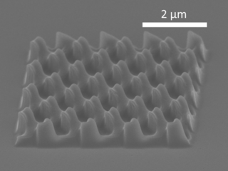
Three-dimensional (3D) microfabrication refers to manufacturing techniques that involve the layering of materials to produce a three-dimensional structure at a microscopic scale. These structures are usually on the scale of micrometers and are popular in microelectronics and microelectromechanical systems.

References

  1. "SU-8 Resists: FAQs". MicroChem. Archived from the original on 17 May 2009. Retrieved 21 Jul 2011.
  2. Liu J, Cai B, Zhu J, et al. (2004). "Process research of high aspect ratio microstructure using SU-8 resist". Microsyst. Technol. 10 (4): 265–8. doi:10.1007/s00542-002-0242-2. S2CID   111062837.
  3. Johnsona DW, Goettertb J, Singhb V, et al. (2012). "SUEX Dry Film Resist – A new Material for High Aspect Ratio Lithography" (PDF). Louisiana State University Proceedings.
  4. Greener J, Li W, Ren J, et al. (February 2010). "Rapid, cost-efficient fabrication of microfluidic reactors in thermoplastic polymers by combining photolithography and hot embossing". Lab on a Chip. 10 (4): 522–4. doi:10.1039/B918834G. PMID   20126695.
  5. Nemani KV, Moodie KL, Brennick JB, et al. (2013). "In vitro and in vivo evaluation of SU-8 biocompatibility". Materials Science and Engineering: C. 33 (7): 4453–9. doi:10.1016/j.msec.2013.07.001. PMC   3843949 . PMID   23910365.
  6. Arscott S (2014). "SU-8 as a material for lab-on-a-chip-based mass spectrometry". Lab on a Chip. 14 (19): 3668–89. doi:10.1039/C4LC00617H. PMID   25029537.
  7. "NANO SU-8: Negative Tone Photoresist - formulations 50-100" (PDF). Microchem.com. 2011. Archived from the original (PDF) on 2012-04-25. Retrieved 12 Jun 2019.
  8. del Campo A, Greiner C (2007). "SU-8: a photoresist for high-aspect-ratio and 3D submicron lithography". J. Micromech. Microeng. 17 (6): R81–R95. doi:10.1088/0960-1317/17/6/R01. S2CID   18148474.
  9. Martinez-Duarte R, Madou M (2011). "SU-8 Pholithography and its impact on microfluidics". In Mitra SK, Chakraborty S (eds.). Microfluidics and Nanofluidics Handbook: Fabrication, Implementation and Applications (1st ed.). New York: CRC Press. pp. 231–268. ISBN   9781138072381.
  10. "SU-8 Developer". Lambers Wiki (Material Safety Data Sheet). 2005. Archived from the original on 11 December 2017. Retrieved 12 Jun 2019.
  11. "SU-8 photosensitive epoxy". 2003. Archived from the original on 30 May 2012. Retrieved 12 Jun 2019.
  12. Melai J, Salm C, Wolters R, et al. (2009). "Qualitative and quantitative characterization of outgassing from SU-8" (PDF). Microelectronic Engineering. 86 (4–6): 761–764. doi:10.1016/j.mee.2008.11.008. S2CID   137789516.
  13. "SU-8 Photoresist Processing" (PDF). engineering.tufts.edu. 2007. Archived from the original (PDF) on 9 November 2009. Retrieved 12 Jun 2019.
  14. 1 2 "SU-8 2000 Permanent Epoxy Negative Photoresist Processing Guidelines" (PDF). Microchem. Archived from the original (PDF) on 15 April 2017.
  15. 1 2 3 4 "SU-8 Functional Polymer". Gersteltec Engineering Solutions. Retrieved 12 Jun 2019.
  16. "SU8". Gersteltec Engineering Solutions. Retrieved 12 Jun 2019.
  17. S. Arscott, ‘The limits of edge bead planarization and surface levelling in spin-coated liquid films', J. Micromech. Microeng.30, 025003, (2020).
  18. 1 2 "SUEX". djmicrolaminates.com. Retrieved 15 Feb 2017.