
Atomic force microscopy (AFM) or scanning force microscopy (SFM) is a very-high-resolution type of scanning probe microscopy (SPM), with demonstrated resolution on the order of fractions of a nanometer, more than 1000 times better than the optical diffraction limit.
Scanning probe microscopy (SPM) is a branch of microscopy that forms images of surfaces using a physical probe that scans the specimen. SPM was founded in 1981, with the invention of the scanning tunneling microscope, an instrument for imaging surfaces at the atomic level. The first successful scanning tunneling microscope experiment was done by Gerd Binnig and Heinrich Rohrer. The key to their success was using a feedback loop to regulate gap distance between the sample and the probe.
Scanning voltage microscopy (SVM), sometimes also called nanopotentiometry, is a scientific experimental technique based on atomic force microscopy. A conductive probe, usually only a few nanometers wide at the tip, is placed in full contact with an operational electronic or optoelectronic sample. By connecting the probe to a high-impedance voltmeter and rastering over the sample's surface, a map of the electric potential can be acquired. SVM is generally nondestructive to the sample although some damage may occur to the sample or the probe if the pressure required to maintain good electrical contact is too high. If the input impedance of the voltmeter is sufficiently large, the SVM probe should not perturb the operation of the operational sample.

A scanning transmission electron microscope (STEM) is a type of transmission electron microscope (TEM). Pronunciation is [stɛm] or [ɛsti:i:ɛm]. As with a conventional transmission electron microscope (CTEM), images are formed by electrons passing through a sufficiently thin specimen. However, unlike CTEM, in STEM the electron beam is focused to a fine spot which is then scanned over the sample in a raster illumination system constructed so that the sample is illuminated at each point with the beam parallel to the optical axis. The rastering of the beam across the sample makes STEM suitable for analytical techniques such as Z-contrast annular dark-field imaging, and spectroscopic mapping by energy dispersive X-ray (EDX) spectroscopy, or electron energy loss spectroscopy (EELS). These signals can be obtained simultaneously, allowing direct correlation of images and spectroscopic data.
Characterization, when used in materials science, refers to the broad and general process by which a material's structure and properties are probed and measured. It is a fundamental process in the field of materials science, without which no scientific understanding of engineering materials could be ascertained. The scope of the term often differs; some definitions limit the term's use to techniques which study the microscopic structure and properties of materials, while others use the term to refer to any materials analysis process including macroscopic techniques such as mechanical testing, thermal analysis and density calculation. The scale of the structures observed in materials characterization ranges from angstroms, such as in the imaging of individual atoms and chemical bonds, up to centimeters, such as in the imaging of coarse grain structures in metals.

Feature-oriented scanning (FOS) is a method of precision measurement of surface topography with a scanning probe microscope in which surface features (objects) are used as reference points for microscope probe attachment. With FOS method, by passing from one surface feature to another located nearby, the relative distance between the features and the feature neighborhood topographies are measured. This approach allows to scan an intended area of a surface by parts and then reconstruct the whole image from the obtained fragments. Beside the mentioned, it is acceptable to use another name for the method – object-oriented scanning (OOS).

Nanometrology is a subfield of metrology, concerned with the science of measurement at the nanoscale level. Nanometrology has a crucial role in order to produce nanomaterials and devices with a high degree of accuracy and reliability in nanomanufacturing.
The following outline is provided as an overview of and topical guide to nanotechnology:
A recurrence tracking microscope (RTM) is a microscope that is based on the quantum recurrence phenomenon of an atomic wave packet. It is used to investigate the nano-structure on a surface.

Piezoresponse force microscopy (PFM) is a variant of atomic force microscopy (AFM) that allows imaging and manipulation of piezoelectric/ferroelectric materials domains. This is achieved by bringing a sharp conductive probe into contact with a ferroelectric surface and applying an alternating current (AC) bias to the probe tip in order to excite deformation of the sample through the converse piezoelectric effect (CPE). The resulting deflection of the probe cantilever is detected through standard split photodiode detector methods and then demodulated by use of a lock-in amplifier (LiA). In this way topography and ferroelectric domains can be imaged simultaneously with high resolution.
The technique of vibrational analysis with scanning probe microscopy allows probing vibrational properties of materials at the submicrometer scale, and even of individual molecules. This is accomplished by integrating scanning probe microscopy (SPM) and vibrational spectroscopy. This combination allows for much higher spatial resolution than can be achieved with conventional Raman/FTIR instrumentation. The technique is also nondestructive, requires non-extensive sample preparation, and provides more contrast such as intensity contrast, polarization contrast and wavelength contrast, as well as providing specific chemical information and topography images simultaneously.
Nanosensors Inc. is a company that manufactures probes for use in atomic force microscopes (AFM) and scanning probe microscopes (SPM). This private, for profit company was founded November 21, 2018. Nanosensors Inc. is located in Neuchatel, Switzerland.

Scanning near-field ultrasound holography (SNFUH) is a method for performing nondestructive nano-scale high-resolution imaging of buried and embedded structures. SNFUH is critical for analysis of materials, structures and phenomena as they continue to shrink at the micro/nano scale. SNFUH is a type of scanning probe microscopy (SPM) technique that provides depth information as well as spatial resolution at the 10 to 100 nm scale.
The Institute for Functional Imaging of Materials (IFIM) is an organization set up in 2014, within the Oak Ridge National Laboratory (ORNL) situated in Oak Ridge, Tennessee, USA. The goal of the institute is to provide a bridge between modeling and applied mathematics and imaging data collected from various forms of microscopy available at ORNL. The current director of the IFIM is Sergei Kalinin who was awarded the Medal for Scanning Probe Microscopy by the Royal Microscopical Society. The institute supports President Obama's Materials Genome Initiative.
A probe tip is an instrument used in scanning probe microscopes (SPMs) to scan the surface of a sample and make nano-scale images of surfaces and structures. The probe tip is mounted on the end of a cantilever and can be as sharp as a single atom. In microscopy, probe tip geometry and the composition of both the tip and the surface being probed directly affect resolution and imaging quality. Tip size and shape are extremely important in monitoring and detecting interactions between surfaces. SPMs can precisely measure electrostatic forces, magnetic forces, chemical bonding, Van der Waals forces, and capillary forces. SPMs can also reveal the morphology and topography of a surface.
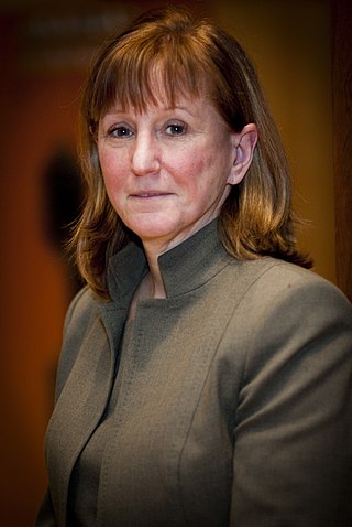
Dawn Austin Bonnell is the Senior Vice Provost for Research at the University of Pennsylvania. She has previously served as the Founding Director of the National Science Foundation Nano–Bio Interface Center, Vice President of the American Ceramic Society and President of the American Vacuum Society. In 2024, she was elected to the American Philosophical Society.
This glossary of nanotechnology is a list of definitions of terms and concepts relevant to nanotechnology, its sub-disciplines, and related fields.

Miaofang Chi is a distinguished scientist at the Center for Nanophase Materials Sciences in Oak Ridge National Laboratory. Her primary research interests are understanding interfacial charge transfer and mass transport behavior in energy and quantum materials and systems by advancing and employing novel electron microscopy techniques, such as in situ and cryogenic scanning transmission electron microscopy. She was awarded the 2016 Microscopy Society of America Burton Medal and the 2019 Microanalysis Society Kurt Heinrich Award. She was named to Clarivate's list of Highly Cited Researchers in 2018 and 2020.
Peter David Nellist, is a British physicist and materials scientist, currently a professor in the Department of Materials at the University of Oxford. He is noted for pioneering new techniques in high-resolution electron microscopy.
