
Semiconductor device fabrication is the process used to manufacture semiconductor devices, typically integrated circuits (ICs) such as computer processors, microcontrollers, and memory chips that are present in everyday electronic devices. It is a multiple-step photolithographic and physio-chemical process during which electronic circuits are gradually created on a wafer, typically made of pure single-crystal semiconducting material. Silicon is almost always used, but various compound semiconductors are used for specialized applications.

A transistor is a semiconductor device used to amplify or switch electrical signals and power. It is one of the basic building blocks of modern electronics. It is composed of semiconductor material, usually with at least three terminals for connection to an electronic circuit. A voltage or current applied to one pair of the transistor's terminals controls the current through another pair of terminals. Because the controlled (output) power can be higher than the controlling (input) power, a transistor can amplify a signal. Some transistors are packaged individually, but many more in miniature form are found embedded in integrated circuits. Because transistors are the key active components in practically all modern electronics, many people consider them one of the 20th century's greatest inventions.
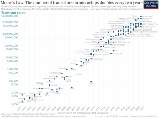
Moore's law is the observation that the number of transistors in an integrated circuit (IC) doubles about every two years. Moore's law is an observation and projection of a historical trend. Rather than a law of physics, it is an empirical relationship linked to gains from experience in production.

EEPROM or E2PROM (electrically erasable programmable read-only memory) is a type of non-volatile memory. It is used in computers, usually integrated in microcontrollers such as smart cards and remote keyless systems, or as a separate chip device, to store relatively small amounts of data by allowing individual bytes to be erased and reprogrammed.
In semiconductor manufacturing, silicon on insulator (SOI) technology is fabrication of silicon semiconductor devices in a layered silicon–insulator–silicon substrate, to reduce parasitic capacitance within the device, thereby improving performance. SOI-based devices differ from conventional silicon-built devices in that the silicon junction is above an electrical insulator, typically silicon dioxide or sapphire. The choice of insulator depends largely on intended application, with sapphire being used for high-performance radio frequency (RF) and radiation-sensitive applications, and silicon dioxide for diminished short-channel effects in other microelectronics devices. The insulating layer and topmost silicon layer also vary widely with application.

A fin field-effect transistor (FinFET) is a multigate device, a MOSFET built on a substrate where the gate is placed on two, three, or four sides of the channel or wrapped around the channel, forming a double or even multi gate structure. These devices have been given the generic name "FinFETs" because the source/drain region forms fins on the silicon surface. The FinFET devices have significantly faster switching times and higher current density than planar CMOS technology.
Aldert van der Ziel, was a Dutch physicist who studied electronic noise processes in materials such as semiconductors and metals.
SONOS, short for "silicon–oxide–nitride–oxide–silicon", more precisely, "polycrystalline silicon"—"silicon dioxide"—"silicon nitride"—"silicon dioxide"—"silicon", is a cross sectional structure of MOSFET (metal–oxide–semiconductor field-effect transistor), realized by P.C.Y. Chen of Fairchild Camera and Instrument in 1977. This structure is often used for non-volatile memories, such as EEPROM and flash memories. It is sometimes used for TFT LCD displays. It is one of CTF (charge trap flash) variants. It is distinguished from traditional non-volatile memory structures by the use of silicon nitride (Si3N4 or Si9N10) instead of "polysilicon-based FG (floating-gate)" for the charge storage material. A further variant is "SHINOS" ("silicon"—"hi-k"—"nitride"—"oxide"—"silicon"), which is substituted top oxide layer with high-κ material. Another advanced variant is "MONOS" ("metal–oxide–nitride–oxide–silicon"). Companies offering SONOS-based products include Cypress Semiconductor, Macronix, Toshiba, United Microelectronics Corporation and Floadia.
The "14 nanometer process" refers to a marketing term for the MOSFET technology node that is the successor to the "22 nm" node. The "14 nm" was so named by the International Technology Roadmap for Semiconductors (ITRS). Until about 2011, the node following "22 nm" was expected to be "16 nm". All "14 nm" nodes use FinFET technology, a type of multi-gate MOSFET technology that is a non-planar evolution of planar silicon CMOS technology.

A multigate device, multi-gate MOSFET or multi-gate field-effect transistor (MuGFET) refers to a metal–oxide–semiconductor field-effect transistor (MOSFET) that has more than one gate on a single transistor. The multiple gates may be controlled by a single gate electrode, wherein the multiple gate surfaces act electrically as a single gate, or by independent gate electrodes. A multigate device employing independent gate electrodes is sometimes called a multiple-independent-gate field-effect transistor (MIGFET). The most widely used multi-gate devices are the FinFET and the GAAFET, which are non-planar transistors, or 3D transistors.
Nanocircuits are electrical circuits operating on the nanometer scale. This is well into the quantum realm, where quantum mechanical effects become very important. One nanometer is equal to 10−9 meters or a row of 10 hydrogen atoms. With such progressively smaller circuits, more can be fitted on a computer chip. This allows faster and more complex functions using less power. Nanocircuits are composed of three different fundamental components. These are transistors, interconnections, and architecture, all fabricated on the nanometer scale.
Chenming Calvin Hu is a Taiwanese-American electronic engineer who specializes in microelectronics. He is TSMC Distinguished Professor Emeritus in the electronic engineering and computer science department of the University of California, Berkeley, in the United States. In 2009, the Institute of Electrical and Electronics Engineers described him as a “microelectronics visionary … whose seminal work on metal-oxide semiconductor MOS reliability and device modeling has had enormous impact on the continued scaling of electronic devices”.
In semiconductor manufacturing, the International Roadmap for Devices and Systems defines the "5 nm" process as the MOSFET technology node following the "7 nm" node. In 2020, Samsung and TSMC entered volume production of "5 nm" chips, manufactured for companies including Apple, Marvell, Huawei and Qualcomm.
The IEEE International Electron Devices Meeting (IEDM) is an annual micro- and nanoelectronics conference held each December that serves as a forum for reporting technological breakthroughs in the areas of semiconductor and related device technologies, design, manufacturing, physics, modeling and circuit-device interaction.
A nanoelectromechanical (NEM) relay is an electrically actuatedswitch that is built on the nanometer scale using semiconductor fabrication techniques. They are designed to operate in replacement of, or in conjunction with, traditional semiconductor logic. While the mechanical nature of NEM relays makes them switch much slower than solid-state relays, they have many advantageous properties, such as zero current leakage and low power consumption, which make them potentially useful in next generation computing.

Beyond CMOS refers to the possible future digital logic technologies beyond the scaling limits of CMOS technology. which limits device density and speeds due to heating effects.

Dr. Gary Patton is an American technologist and business executive. He is currently the Corporate Vice President and General Manager of Design Enablement and Components Research in the Technology Development Group at Intel. He has spent most of his career in IBM, starting in IBM's Research Division and holding management and executive positions in IBM's Microelectronics Division in Technology Development, Design Enablement, Manufacturing, and Business Line Management.
In semiconductor manufacturing, the "2 nm process" is the next MOSFET die shrink after the "3 nm" process node.

Costas J. Spanos is the Director of the Center for Information Technology Research in the Interest of Society (CITRIS) at UC Berkeley. He is also the CEO of the Berkeley Educational Alliance for Research in Singapore (BEARS) and the Andrew S. Grove Distinguished Professor of Electrical Engineering and Computer Sciences (EECS) at UC Berkeley.
