Avalanche transistor

Last updated

An avalanche transistor is a bipolar junction transistor designed for operation in the region of its collector-current/collector-to-emitter voltage characteristics beyond the collector-to-emitter breakdown voltage, called avalanche breakdown region. This region is characterized by avalanche breakdown, which is a phenomenon similar to Townsend discharge for gases, and negative differential resistance. Operation in the avalanche breakdown region is called avalanche-mode operation: it gives avalanche transistors the ability to switch very high currents with less than a nanosecond rise and fall times (transition times). Transistors not specifically designed for the purpose can have reasonably consistent avalanche properties; for example 82% of samples of the 15V high-speed switch 2N2369, manufactured over a 12-year period, were capable of generating avalanche breakdown pulses with rise time of 350 ps or less, using a 90V power supply as Jim Williams writes. [1] [2]

Contents

History

The first paper dealing with avalanche transistors was Ebers & Miller (1955). The paper describes how to use alloy-junction transistors in the avalanche breakdown region in order to overcome speed and breakdown voltage limitations which affected the first models of such kind of transistor when used in earlier computer digital circuits. Therefore, the very first applications of avalanche transistors were in switching circuits and multivibrators. The introduction of the avalanche transistor served also as an application of Miller's empirical formula for the avalanche multiplication coefficient , first introduced in the paper Miller (1955). The need for better understanding transistor behavior in the avalanche breakdown region, not only for use in avalanche mode, gave rise to an extensive research on impact ionization in semiconductors (see Kennedy & O'Brien (1966)).

From the beginning of the 1960s to the first half of the 1970s, several avalanche-transistor circuits were proposed. The kind of bipolar junction transistor best suited for use in the avalanche breakdown region was studied. A complete reference, which includes also the contributions of scientists from ex-USSR and COMECON countries, is the book by Дьяконов (Dyakonov) (1973).

The first application of the avalanche transistor as a linear amplifier, named Controlled Avalanche Transit Time Triode, (CATT) was described in ( Eshbach, Se Puan & Tantraporn 1976 ). A similar device, named IMPISTOR was described more or less in the same period in the paper of Carrol & Winstanley (1974). Linear applications of this class of devices started later since there are some requirements to fulfill, as described below. The use of avalanche transistors in those applications is not mainstream since the devices require high collector to emitter voltages in order to work properly.

Nowadays, there is still active research on avalanche devices (transistors or other) made of compound semiconductors, capable of switching currents of several tens of amperes even faster than "traditional" avalanche transistors.

Basic theory

Static avalanche region characteristics

Bias currents and voltages for an NPN bipolar transistor Bias currents and voltages for an NPN bipolar transistor.png
Bias currents and voltages for an NPN bipolar transistor

In this section, the static characteristic of an avalanche transistor is calculated. For the sake of simplicity, only an NPN device is considered: however, the same results are valid for PNP devices only changing signs to voltages and currents accordingly. The analysis closely follows that of William D. Roehr in ( Roehr 1963 ). Since avalanche breakdown multiplication is present only across the collector-base junction, the first step of the calculation is to determine collector current as a sum of various component currents though the collector since only those fluxes of charge are subject to this phenomenon. Kirchhoff's current law applied to a bipolar junction transistor implies the following relation, always satisfied by the collector current

while for the same device working in the active region, basic transistor theory gives the following relation

where

Equating the two formulas for gives the following result

and since is the common base current gain of the transistor, then

When avalanche effects in a transistor collector are considered, the collector current is given by

where is Miller's avalanche multiplication coefficient. It is the most important parameter in avalanche mode operation: its expression is the following

where

Using again Kirchhoff's current law for the bipolar junction transistor and the given expression for , the resulting expression for is the following

and remembering that and where is the base-emitter voltage

since : this is the expression of the parametric family of the collector characteristics with parameter . Note that increases without limit if

where is the collector-emitter breakdown voltage. Also, it is possible to express as a function of , and obtain an analytical formula for the collector-emitter differential resistance by straightforward differentiation: however, the details are not given here.

Differential dynamical model

Equivalent circuit of an avalanche npn bipolar transistor operated by a commonly used bias network. Avalanche BJT equiv circ-1.png
Equivalent circuit of an avalanche npn bipolar transistor operated by a commonly used bias network.

The differential dynamical mode described here, also called the small signal model, is the only intrinsic small signal model of the avalanche transistor. Stray elements due to the package enclosing the transistor are deliberately neglected, since their analysis would not add anything useful from the point of view of the working principles of the avalanche transistor. However, when realizing an electronic circuit, those parameters are of great importance. Particularly, stray inductances in series with collector and emitter leads have to be minimized to preserve the high speed performance of avalanche transistor circuits. Also, this equivalent circuit is useful when describing the behavior of the avalanche transistor near its turn on time, where collector currents and voltages are still near their quiescent values: in the real circuit it permits the calculation of time constants and therefore rise and fall times of the waveform. However, since avalanche transistor switching circuits are intrinsically large signal circuits, the only way to predict with reasonable accuracy their real behaviour is to do numerical simulations. Again, the analysis closely follows that of William D. Roehr in ( Roehr 1963 ).

An avalanche transistor operated by a common bias network is shown in the adjacent picture: can be zero or positive value, while can be short circuited. In every avalanche transistor circuit, the output signal is taken from the collector or the emitter: therefore the small-signal differential model of an avalanche transistor working in the avalanche region is always seen from the collector-emitter output pins, and consist of a parallel circuit as shown in the adjacent picture, which includes only bias components. The magnitude and sign of both those parameters are controlled by the base current : since both base-collector and base-emitter junctions are inversely biased in the quiescent state, the equivalent circuit of the base input is simply a current generator shunted by base-emitter and base-collector junction capacitances and is therefore not analyzed in what follows. The intrinsic time constant of the basic equivalent small signal circuit has the following value

where

where
is the current gain angular cutoff frequency
is the common base output capacitance

The two parameters are both negative. This means that if the collector load const of an ideal current source, the circuit is unstable. This is the theoretical justification of the astable multivibrator behavior of the circuit when the voltage is raised over some critical level.

Second breakdown avalanche mode

When the collector current rises above the data sheet limit a new breakdown mechanism become important: the second breakdown. This phenomenon is caused by excessive heating of some points (hot spots) in the base-emitter region of the bipolar junction transistor, which give rise to an exponentially increasing current through these points: this exponential rise of current in turn gives rise to even more overheating, originating a positive thermal feedback mechanism. While analyzing the static characteristic, the presence of this phenomenon is seen as a sharp collector voltage drop and a corresponding almost vertical rise of the collector current. At the present, it is not possible to produce a transistor without hot spots and thus without second breakdown, since their presence is related to the technology of refinement of silicon. During this process, very small but finite quantities of metals remain in localized portions of the wafer: these particles of metals became deep centers of recombination, i.e. centers where current exists in a preferred way. While this phenomenon is destructive for Bipolar junction transistors working in the usual way, it can be used to push-up further the current and voltage limits of a device working in avalanche mode by limiting its time duration: also, the switching speed of the device is not negatively affected. A clear description of avalanche transistor circuits working in second breakdown regime together with some examples can be found in the paper Baker (1991).

Numerical simulations

Avalanche transistor circuits are intrinsically large signal circuits, so small signal models, when applied to such circuits, can only give a qualitative description. To obtain more accurate information about the behavior of time dependent voltages and currents in such circuits it is necessary to use numerical analysis. The "classical" approach, detailed in the paper Дьяконов (Dyakonov) (2004b) which relies upon the book Дьяконов (Dyakonov) (1973), consists in considering the circuits as a system of nonlinear ordinary differential equations and solve it by a numerical method implemented by a general purpose numerical simulation software: results obtained in this way are fairly accurate and simple to obtain. However, these methods rely on the use of analytical transistor models best suited for the analysis of the breakdown region: those models are not necessarily suited to describe the device working in all possible regions. A more modern approach is to use the common analog circuit simulator SPICE together with an advanced transistor model supporting avalanche breakdown simulations, which the basic SPICE transistor model does not. Examples of such models are described in the paper Keshavarz, Raney & Campbell (1993) and in the paper Kloosterman & De Graaff (1989): the latter is a description of the Mextram model, currently used by some semiconductor industries to characterize their bipolar junction transistors.

A graphical method

A graphical method for studying the behavior of an avalanche transistor was proposed in references Spirito (1968) and Spirito (1971): the method was first derived in order to plot the static behavior of the device and then was applied also to solve problems concerning the dynamic behavior. The method bears the spirit of the graphical methods used to design tube and transistor circuits directly from the characteristic diagrams given in data sheets by producers.

Applications

Avalanche transistors are mainly used as fast pulse generators, having rise and fall times of less than a nanosecond and high output voltage and current. They are occasionally used as amplifiers in the microwave frequency range, even if this use is not mainstream: when used for this purpose, they are called "Controlled Avalanche Transit-time Triodes" (CATTs).

Avalanche mode switching circuits

Avalanche mode switching relies on avalanche multiplication of current flowing through the collector-base junction as a result of impact ionization of the atoms in the semiconductor crystal lattice. Avalanche breakdown in semiconductors has found application in switching circuits for two basic reasons

The two circuits considered in this section are the simplest examples of avalanche transistor circuits for switching purposes: both the examples detailed are monostable multivibrators. There are several more complex circuits in the literature, for example in the books Roehr (1963) and Дьяконов (Dyakonov) (1973).

Most circuits employing an avalanche transistor are activated by the following two different kinds of input:

Simplified collector trigger circuit of an avalanche npn bipolar transistor operated by a commonly used bias network. Avalanche bjt collector trigger.png
Simplified collector trigger circuit of an avalanche npn bipolar transistor operated by a commonly used bias network.
Simplified base trigger circuit of an avalanche npn bipolar transistor operated by a commonly used bias network. Avalanche bjt base trigger.png
Simplified base trigger circuit of an avalanche npn bipolar transistor operated by a commonly used bias network.

Avalanche transistor can also be triggered by lowering the emitter voltage , but this configuration is rarely seen in the literature and in practical circuits.: in reference Meiling & Stary (1968), paragraph 3.2.4 "Trigger circuits" one such configuration is described, where the avalanche transistor is used itself as a part of the trigger circuit of a complex pulser, while in reference Дьяконов (Dyakonov) (1973 , pp. 185) a balanced level discriminator where a common bipolar junction transistor is emitter-coupled to an avalanche transistor is briefly described.

The two avalanche pulser described below are both base triggered and have two outputs. Since the device used is an NPN transistor, is a positive going output while is a negative going output: using a PNP transistor reverses the polarities of outputs. The description of their simplified versions, where resistor or is set to zero ohm (obviously not both) in order to have a single output, can be found in reference Millman & Taub (1965). Resistor recharges the capacitor or the transmission line (i.e. the energy storage components) after commutation. It has usually a high resistance to limit the static collector current, so the recharging process is slow. Sometimes this resistor is replaced by an electronic circuit which is capable of charging faster the energy storage components.

In practical designs, an adjustable impedance like a two terminal Zobel network (or simply a trimmer capacitor) is placed from the collector of the avalanche transistor to ground, giving the transmission line pulser the ability to reduce ringing and other undesired behavior on the output voltages.

Simplified capacitor discharge avalanche transistor pulser. Avalanche bjt capacitor discharge pulser.png
Simplified capacitor discharge avalanche transistor pulser.
Simplified transmission line avalanche transistor pulser. Avalanche bjt transmission line pulser.png
Simplified transmission line avalanche transistor pulser.

It is possible to turn those circuits into astable multivibrators by removing their trigger input circuits and

  1. raising their power supply voltage until a relaxation oscillation begins, or
  2. connecting the base resistor to a positive base bias voltage and thus forcibly starting avalanche breakdown and associated relaxation oscillation.

A well-detailed example of the first procedure is described in reference Holme (2006). It is also possible to realize avalanche mode bistable multivibrators, but their use is not as common as other types described of multivibrators, one important reason being that they require two avalanche transistors, one working continuously in avalanche breakdown regime, and this can give serious problems from the point of view of power dissipation and device operating life.

A practical, easily realised, and inexpensive application is the generation of fast-rising pulses for checking equipment rise time. [1] [3]

The controlled avalanche transit-time triode (CATT)

Avalanche mode amplification relies on avalanche multiplication as avalanche mode switching. However, for this mode of operation, it is necessary that Miller's avalanche multiplication coefficient be kept almost constant for large output voltage swings: if this condition is not fulfilled, significant amplitude distortion arises on the output signal. Consequently,

These two requirements imply that a device used for amplification need a physical structure different from that of a typical avalanche transistor. The Controlled Avalanche Transit-time Triode (CATT), designed for microwave amplification, has a quite large lightly-doped region between the base and the collector regions, giving the device a collector-emitter breakdown voltage fairly high compared to bipolar transistors of the same geometry. The current amplification mechanism is the same of the avalanche transistor, i.e. carrier generation by impact ionization, but there is also a transit-time effect as in IMPATT and TRAPATT diodes, where a high-field region travels along the avalanching junction, precisely in along the intrinsic region. The device structure and choice of bias point imply that

  1. Miller's avalanche multiplication coefficient M is limited to about 10.
  2. The transit-time effect keeps this coefficient almost constant and independent of the collector-to-emitter voltage.

The theory for this kind of avalanche transistor is described completely in the paper Eshbach, Se Puan & Tantraporn (1976), which also shows that this semiconductor device structure is well suited for microwave power amplification. It can deliver several watts of radio frequency power at a frequency of several gigahertz and it also has a control terminal, the base. However, it is not widely used since it requires voltages exceeding 200 volts to work properly, while gallium arsenide or other compound semiconductor FETs deliver a similar performance while being easier to work with. A similar device structure, proposed more or less in the same period in the paper Carrol & Winstanley (1974), was the IMPISTOR, being a transistor with IMPATT collector-base junction.

Schematic of a CATT microwave amplifier. CATT amplifier.png
Schematic of a CATT microwave amplifier.

See also

Notes

  1. 1 2 "Linear Technology AN47" Archived March 20, 2012, at the Wayback Machine , High-speed amplifier techniques, 1991, Appendix D: Measuring probe-oscilloscope response.
  2. "Linear Technology AN94", Slew Rate Verification for Wideband Amplifiers The Taming of the Slew"
  3. iceNINE Tech: Homebrew Really Fast Pulse Generator

Related Research Articles

<span class="mw-page-title-main">Multivibrator</span> Electronic circuit used to implement two-state devices

A multivibrator is an electronic circuit used to implement a variety of simple two-state devices such as relaxation oscillators, timers, latches and flip-flops. The first multivibrator circuit, the astable multivibrator oscillator, was invented by Henri Abraham and Eugene Bloch during World War I. It consisted of two vacuum tube amplifiers cross-coupled by a resistor-capacitor network. They called their circuit a "multivibrator" because its output waveform was rich in harmonics. A variety of active devices can be used to implement multivibrators that produce similar harmonic-rich wave forms; these include transistors, neon lamps, tunnel diodes and others. Although cross-coupled devices are a common form, single-element multivibrator oscillators are also common.

<span class="mw-page-title-main">Transistor</span> Solid-state electrically operated switch also used as an amplifier

A transistor is a semiconductor device used to amplify or switch electrical signals and power. It is one of the basic building blocks of modern electronics. It is composed of semiconductor material, usually with at least three terminals for connection to an electronic circuit. A voltage or current applied to one pair of the transistor's terminals controls the current through another pair of terminals. Because the controlled (output) power can be higher than the controlling (input) power, a transistor can amplify a signal. Some transistors are packaged individually, but many more in miniature form are found embedded in integrated circuits. Because transistors are the key active components in practically all modern electronics, many people consider them one of the 20th century's greatest inventions.

<span class="mw-page-title-main">Photodiode</span> Converts light into current

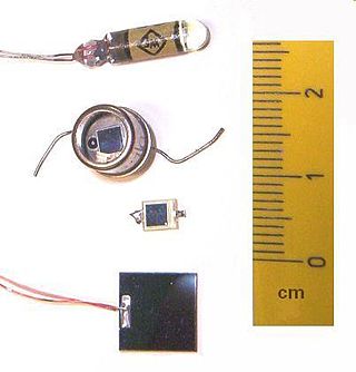
A photodiode is a semiconductor diode sensitive to photon radiation, such as visible light, infrared or ultraviolet radiation, X-rays and gamma rays. Photodiode is a PN semiconductor material that produces current or voltage Photovoltaics when it absorbs photons Semiconductor Optoelectronics . The physics of electron excitation for photodiodes are similar to Photoconductivity typically implemented as a Photoresistor or as switches in Thyristor#Photothyristors. Photodiodes can be used for detection and measurement applications, or optimized for the generation of electrical power in solar cells. Photodiodes are used in a wide range of applications throughout the electromagnetic spectrum from IR, visible light, UV photocells to gamma ray spectrometers.

<span class="mw-page-title-main">Bipolar junction transistor</span> Transistor that uses both electrons and holes as charge carriers

A bipolar junction transistor (BJT) is a type of transistor that uses both electrons and electron holes as charge carriers. In contrast, a unipolar transistor, such as a field-effect transistor (FET), uses only one kind of charge carrier. A bipolar transistor allows a small current injected at one of its terminals to control a much larger current flowing between the terminals, making the device capable of amplification or switching.

<span class="mw-page-title-main">Zener diode</span> Diode that allows current to flow in the reverse direction at a specific voltage

A Zener diode is a special type of diode designed to reliably allow current to flow "backwards" when a certain set reverse voltage, known as the Zener voltage, is reached.

A unijunction transistor (UJT) is a three-lead electronic semiconductor device with only one junction. It acts exclusively as an electrically controlled switch.

<span class="mw-page-title-main">Insulated-gate bipolar transistor</span> Type of solid state switch

An insulated-gate bipolar transistor (IGBT) is a three-terminal power semiconductor device primarily forming an electronic switch. It was developed to combine high efficiency with fast switching. It consists of four alternating layers (P–N–P–N) that are controlled by a metal–oxide–semiconductor (MOS) gate structure.

<span class="mw-page-title-main">555 timer IC</span> Integrated circuit used for timer applications

The 555 timer IC is an integrated circuit used in a variety of timer, delay, pulse generation, and oscillator applications. It is one of the most popular timing ICs due to its flexibility and price. Derivatives provide two or four timing circuits in one package. The design was first marketed in 1972 by Signetics and used bipolar junction transistors. Since then, numerous companies have made the original timers and later similar low-power CMOS timers. In 2017, it was said that over a billion 555 timers are produced annually by some estimates, and that the design was "probably the most popular integrated circuit ever made".

A current mirror is a circuit designed to copy a current through one active device by controlling the current in another active device of a circuit, keeping the output current constant regardless of loading. The current being "copied" can be, and sometimes is, a varying signal current. Conceptually, an ideal current mirror is simply an ideal inverting current amplifier that reverses the current direction as well, or it could consist of a current-controlled current source (CCCS). The current mirror is used to provide bias currents and active loads to circuits. It can also be used to model a more realistic current source.

p–n junction Semiconductor–semiconductor junction

A p–n junction is a boundary or interface between two types of semiconductor materials, p-type and n-type, inside a single crystal of semiconductor. The "p" (positive) side contains an excess of holes, while the "n" (negative) side contains an excess of electrons in the outer shells of the electrically neutral atoms there. This allows electric current to pass through the junction only in one direction. The p- and n-type regions creating the junction are made by doping the semiconductor, for example by ion implantation, diffusion of dopants, or by epitaxy.

<span class="mw-page-title-main">Current source</span> Electronic component delivering stable electric current regardless of voltage

A current source is an electronic circuit that delivers or absorbs an electric current which is independent of the voltage across it.

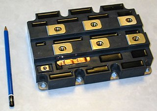
A power semiconductor device is a semiconductor device used as a switch or rectifier in power electronics. Such a device is also called a power device or, when used in an integrated circuit, a power IC.

<span class="mw-page-title-main">Single-photon avalanche diode</span> Solid-state photodetector

A single-photon avalanche diode (SPAD), also called Geiger-mode avalanche photodiode is a solid-state photodetector within the same family as photodiodes and avalanche photodiodes (APDs), while also being fundamentally linked with basic diode behaviours. As with photodiodes and APDs, a SPAD is based around a semi-conductor p-n junction that can be illuminated with ionizing radiation such as gamma, x-rays, beta and alpha particles along with a wide portion of the electromagnetic spectrum from ultraviolet (UV) through the visible wavelengths and into the infrared (IR).

<span class="mw-page-title-main">Safe operating area</span> Technical specification

For power semiconductor devices, the safe operating area (SOA) is defined as the voltage and current conditions over which the device can be expected to operate without self-damage.

<span class="mw-page-title-main">Breakdown voltage</span> Voltage at which insulator becomes conductive

The breakdown voltage of an insulator is the minimum voltage that causes a portion of an insulator to experience electrical breakdown and become electrically conductive.

<span class="mw-page-title-main">Power MOSFET</span> MOSFET that can handle significant power levels

A power MOSFET is a specific type of metal–oxide–semiconductor field-effect transistor (MOSFET) designed to handle significant power levels. Compared to the other power semiconductor devices, such as an insulated-gate bipolar transistor (IGBT) or a thyristor, its main advantages are high switching speed and good efficiency at low voltages. It shares with the IGBT an isolated gate that makes it easy to drive. They can be subject to low gain, sometimes to a degree that the gate voltage needs to be higher than the voltage under control.

A Wilson current mirror is a three-terminal circuit that accepts an input current at the input terminal and provides a "mirrored" current source or sink output at the output terminal. The mirrored current is a precise copy of the input current. It may be used as a Wilson current source by applying a constant bias current to the input branch as in Fig. 2. The circuit is named after George R. Wilson, an integrated circuit design engineer who worked for Tektronix. Wilson devised this configuration in 1967 when he and Barrie Gilbert challenged each other to find an improved current mirror overnight that would use only three transistors. Wilson won the challenge.

<span class="mw-page-title-main">Early effect</span> Variation in the effective width of the base in a bipolar junction transistor

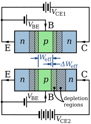
The Early effect, named after its discoverer James M. Early, is the variation in the effective width of the base in a bipolar junction transistor (BJT) due to a variation in the applied base-to-collector voltage. A greater reverse bias across the collector–base junction, for example, increases the collector–base depletion width, thereby decreasing the width of the charge carrier portion of the base.

<span class="mw-page-title-main">Bipolar transistor biasing</span> Process necessary for BJT amplifiers to work correctly

Bipolar transistors must be properly biased to operate correctly. In circuits made with individual devices, biasing networks consisting of resistors are commonly employed. Much more elaborate biasing arrangements are used in integrated circuits, for example, bandgap voltage references and current mirrors. The voltage divider configuration achieves the correct voltages by the use of resistors in certain patterns. By selecting the proper resistor values, stable current levels can be achieved that vary only little over temperature and with transistor properties such as β.

<span class="mw-page-title-main">Noise generator</span> Circuit that produces electrical noise

A noise generator is a circuit that produces electrical noise. Noise generators are used to test signals for measuring noise figure, frequency response, and other parameters. Noise generators are also used for generating random numbers.

References

Bibliography

Theory

Applications

Varia