Multivibrator

Last updated

A multivibrator is an electronic circuit used to implement a variety of simple two-state [1] [2] [3] devices such as relaxation oscillators, timers, latches and flip-flops. The first multivibrator circuit, the astable multivibrator oscillator, was invented by Henri Abraham and Eugene Bloch during World War I. It consisted of two vacuum tube amplifiers cross-coupled by a resistor-capacitor network. [4] [5] They called their circuit a "multivibrator" because its output waveform was rich in harmonics. [6] A variety of active devices can be used to implement multivibrators that produce similar harmonic-rich wave forms; these include transistors, neon lamps, tunnel diodes and others. Although cross-coupled devices are a common form, single-element multivibrator oscillators are also common.

Contents

The three types of multivibrator circuits are:

Original vacuum tube Abraham-Bloch multivibrator oscillator, from their 1919 paper Original Abraham-Bloch multivibrator circuit.png
Original vacuum tube Abraham-Bloch multivibrator oscillator, from their 1919 paper
  1. Astable multivibrator, in which the circuit is not stable in either state —it continually switches from one state to the other. It functions as a relaxation oscillator.
  2. Monostable multivibrator, in which one of the states is stable, but the other state is unstable (transient). A trigger pulse causes the circuit to enter the unstable state. After entering the unstable state, the circuit will return to the stable state after a set time. Such a circuit is useful for creating a timing period of fixed duration in response to some external event. This circuit is also known as a one shot.
  3. Bistable multivibrator, in which the circuit is stable in either state. It can be flipped from one state to the other by an external trigger pulse. This circuit is also known as a flip-flop or latch. It can store one bit of information, and is widely used in digital logic and computer memory.

Multivibrators find applications in a variety of systems where square waves or timed intervals are required. For example, before the advent of low-cost integrated circuits, chains of multivibrators found use as frequency dividers.[ citation needed ] A free-running multivibrator with a frequency of one-half to one-tenth of the reference frequency would accurately lock to the reference frequency. This technique was used in early electronic organs, to keep notes of different octaves accurately in tune. Other applications included early television systems, where the various line and frame frequencies were kept synchronized by pulses included in the video signal.

History

A vacuum tube Abraham-Bloch multivibrator oscillator, France, 1920 (small box, left). Its harmonics are being used to calibrate a wavemeter (center). Vacuum tube multivibrator calibrating wavemeter 1920.jpg
A vacuum tube Abraham-Bloch multivibrator oscillator, France, 1920 (small box, left). Its harmonics are being used to calibrate a wavemeter (center).

The first multivibrator circuit, the classic astable multivibrator oscillator (also called a plate-coupled multivibrator) was first described by Henri Abraham and Eugene Bloch in Publication 27 of the French Ministère de la Guerre, and in Annales de Physique 12, 252 (1919). Since it produced a square wave, in contrast to the sine wave generated by most other oscillator circuits of the time, its output contained many harmonics above the fundamental frequency, which could be used for calibrating high frequency radio circuits. For this reason Abraham and Bloch called it a multivibrateur. It is a predecessor of the Eccles-Jordan trigger [7] which was derived from the circuit a year later.

Historically, the terminology of multivibrators has been somewhat variable:

Astable

An astable multivibrator consists of two amplifying stages connected in a positive feedback loop by two capacitive-resistive coupling networks.[ failed verification ] The amplifying elements may be junction or field-effect transistors, vacuum tubes, operational amplifiers, or other types of amplifier. Figure 1, below right, shows bipolar junction transistors.

The circuit is usually drawn in a symmetric form as a cross-coupled pair. The two output terminals can be defined at the active devices and have complementary states. One has high voltage while the other has low voltage, except during the brief transitions from one state to the other.

Operation

The circuit has two astable (unstable) states that change alternatively with maximum transition rate because of the "accelerating" positive feedback. It is implemented by the coupling capacitors that instantly transfer voltage changes because the voltage across a capacitor cannot suddenly change. In each state, one transistor is switched on and the other is switched off. Accordingly, one fully charged capacitor discharges (reverse charges) slowly thus converting the time into an exponentially changing voltage. At the same time, the other empty capacitor quickly charges thus restoring its charge (the first capacitor acts as a time-setting capacitor and the second prepares to play this role in the next state). The circuit operation is based on the fact that the forward-biased base-emitter junction of the switched-on bipolar transistor can provide a path for the capacitor restoration.

State 1 (Q1 is switched on, Q2 is switched off)

In the beginning, the capacitor C1 is fully charged (in the previous State 2) to the power supply voltage V with the polarity shown in Figure 1. Q1 is on and connects the left-hand positive plate of C1 to ground. As its right-hand negative plate is connected to Q2 base, a maximum negative voltage (-V) is applied to Q2 base that keeps Q2 firmly off. C1 begins discharging (reverse charging) via the high-value base resistor R2, so that the voltage of its right-hand plate (and at the base of Q2) is rising from below ground (-V) toward +V. As Q2 base-emitter junction is reverse-biased, it does not conduct, so all the current from R2 goes into C1. Simultaneously, C2 that is fully discharged and even slightly charged to 0.6 V (in the previous State 2) quickly charges via the low-value collector resistor R4 and Q1 forward-biased base-emitter junction (because R4 is less than R2, C2 charges faster than C1). Thus C2 restores its charge and prepares for the next State C2 when it will act as a time-setting capacitor. Q1 is firmly saturated in the beginning by the "forcing" C2 charging current added to R3 current. In the end, only R3 provides the needed input base current. The resistance R3 is chosen small enough to keep Q1 (not deeply) saturated after C2 is fully charged.

Figure 1: Basic BJT astable multivibrator Transistor Multivibrator.svg
Figure 1: Basic BJT astable multivibrator

When the voltage of C1 right-hand plate (Q2 base voltage) becomes positive and reaches 0.6 V, Q2 base-emitter junction begins diverting a part of R2 charging current. Q2 begins conducting and this starts the avalanche-like positive feedback process as follows. Q2 collector voltage begins falling; this change transfers through the fully charged C2 to Q1 base and Q1 begins cutting off. Its collector voltage begins rising; this change transfers back through the almost empty C1 to Q2 base and makes Q2 conduct more thus sustaining the initial input impact on Q2 base. Thus the initial input change circulates along the feedback loop and grows in an avalanche-like manner until finally Q1 switches off and Q2 switches on. The forward-biased Q2 base-emitter junction fixes the voltage of C1 right-hand plate at 0.6 V and does not allow it to continue rising toward +V.

State 2 (Q1 is switched off, Q2 is switched on)

Now, the capacitor C2 is fully charged (in the previous State 1) to the power supply voltage V with the polarity shown in Figure 1. Q2 is on and connects the right-hand positive plate of C2 to ground. As its left-hand negative plate is connected to Q1 base, a maximum negative voltage (-V) is applied to Q1 base that keeps Q1 firmly off. C2 begins discharging (reverse charging) via the high-value base resistor R3, so that the voltage of its left-hand plate (and at the base of Q1) is rising from below ground (-V) toward +V. Simultaneously, C1 that is fully discharged and even slightly charged to 0.6 V (in the previous State 1) quickly charges via the low-value collector resistor R1 and Q2 forward-biased base-emitter junction (because R1 is less than R3, C1 charges faster than C2). Thus C1 restores its charge and prepares for the next State 1 when it will act again as a time-setting capacitor...and so on... (the next explanations are a mirror copy of the second part of State 1).

Multivibrator frequency

Derivation

The duration of state 1 (low output) will be related to the time constant R2C1 as it depends on the charging of C1, and the duration of state 2 (high output) will be related to the time constant R3C2 as it depends on the charging of C2. Because they do not need to be the same, an asymmetric duty cycle is easily achieved.

The voltage on a capacitor with non-zero initial charge is:

Looking at C2, just before Q2 turns on, the left terminal of C2 is at the base-emitter voltage of Q1 (VBE_Q1) and the right terminal is at VCC ("VCC" is used here instead of "+V" to ease notation). The voltage across C2 is VCC minus VBE_Q1 . The moment after Q2 turns on, the right terminal of C2 is now at 0 V which drives the left terminal of C2 to 0 V minus (VCC - VBE_Q1) or VBE_Q1 - VCC. From this instant in time, the left terminal of C2 must be charged back up to VBE_Q1. How long this takes is half our multivibrator switching time (the other half comes from C1). In the charging capacitor equation above, substituting:

VBE_Q1 for
(VBE_Q1 - VCC) for
VCC for

results in:

Solving for t results in:

For this circuit to work, VCC>>VBE_Q1 (for example: VCC=5 V, VBE_Q1=0.6 V), therefore the equation can be simplified to:

or
or

The period of each half of the multivibrator is therefore given by t = ln(2)RC.

The total period of oscillation is given by:

T = t1 + t2 = ln(2)R2C1 + ln(2)R3C2

where...

  • f is frequency in hertz.
  • R2 and R3 are resistor values in ohms.
  • C1 and C2 are capacitor values in farads.
  • T is the period (In this case, the sum of two period durations).

For the special case where

  • t1 = t2 (50% duty cycle)
  • R2 = R3
  • C1 = C2

[13]

Output pulse shape

The output voltage has a shape that approximates a square waveform. It is considered below for the transistor Q1.

During State 1, Q2 base-emitter junction is reverse-biased and capacitor C1 is "unhooked" from ground. The output voltage of the switched-on transistor Q1 changes rapidly from high to low since this low-resistive output is loaded by a high impedance load (the series connected capacitor C1 and the high-resistive base resistor R2).

During State 2, Q2 base-emitter junction is forward-biased and capacitor C1 is "hooked" to ground. The output voltage of the switched-off transistor Q1 changes exponentially from low to high since this relatively high resistive output is loaded by a low impedance load (capacitor C1). This is the output voltage of R1C1 integrating circuit.

To approach the needed square waveform, the collector resistors have to be low in resistance. The base resistors have to be low enough to make the transistors saturate in the end of the restoration (RB < β.RC).

Initial power-up

When the circuit is first powered up, neither transistor will be switched on. However, this means that at this stage they will both have high base voltages and therefore a tendency to switch on, and inevitable slight asymmetries will mean that one of the transistors is first to switch on. This will quickly put the circuit into one of the above states, and oscillation will ensue. In practice, oscillation always occurs for practical values of R and C.

However, if the circuit is temporarily held with both bases high, for longer than it takes for both capacitors to charge fully, then the circuit will remain in this stable state, with both bases at 0.60 V, both collectors at 0 V, and both capacitors charged backwards to −0.60 V. This can occur at startup without external intervention, if R and C are both very small.

Frequency divider

An astable multivibrator can be synchronized to an external chain of pulses. A single pair of active devices can be used to divide a reference by a large ratio, however, the stability of the technique is poor owing to the variability of the power supply and the circuit elements. A division ratio of 10, for example, is easy to obtain but not dependable. Chains of bistable flip-flops provide more predictable division, at the cost of more active elements. [13]

Protective components

While not fundamental to circuit operation, diodes connected in series with the base or emitter of the transistors are required to prevent the base-emitter junction being driven into reverse breakdown when the supply voltage is in excess of the Veb breakdown voltage, typically around 5-10 volts for general purpose silicon transistors. In the monostable configuration, only one of the transistors requires protection.

Astable Multivibrator using Op-Amp circuit Astable multivibrator using OpAmp.svg
Astable Multivibrator using Op-Amp circuit

Astable multivibrator using an op-amp

Assume all the capacitors to be discharged at first. The output of the op-amp Vo at node c is +Vsat initially. At node a, a voltage of +β Vsat is formed due to voltage division where . The current that flows from nodes c and b to ground charges the capacitor C towards +Vsat. During this charging period, the voltage at b becomes greater than +β Vsat at some point. The voltage at inverting terminal will be greater than the voltage at the non-inverting terminal of the op-amp. This is a comparator circuit and hence, the output becomes -Vsat. The voltage at node a becomes -βVsat due to voltage division. Now the capacitor discharges towards -Vsat. At some point, the voltage at b becomes less than -β Vsat. The voltage at the non-inverting terminal will be greater than the voltage at the inverting terminal of the op-amp. So, the output of the op-amp is +Vsat. This repeats and forms a free-running oscillator or an astable multivibrator.

If VC is the voltage across the capacitor and from the graph, the time period of the wave formed at capacitor and the output would match, then the time period could be calculated in this way:

Graph showing the output waveform of the Op-Amp and the waveform formed across the capacitor C. Astable Multivibrator using Op-Amp Graph.jpg
Graph showing the output waveform of the Op-Amp and the waveform formed across the capacitor C.

At t =T1,

Upon solving, we get:

We are taking values of R, C and β such that we get a symmetrical square wave. Thus, we get T1 = T2 and total time period T = T1 + T2. So, the time period of the square wave generated at the output is:

Monostable

Figure 2: Basic BJT monostable multivibrator Transistor Monostable.svg
Figure 2: Basic BJT monostable multivibrator

In the monostable multivibrator, one resistive-capacitive network (C2-R3 in Figure 1) is replaced by a resistive network (just a resistor). The circuit can be thought as a 1/2 astable multivibrator. Q2 collector voltage is the output of the circuit (in contrast to the astable circuit, it has a perfect square waveform since the output is not loaded by the capacitor).

When triggered by an input pulse, a monostable multivibrator will switch to its unstable position for a period of time, and then return to its stable state. The time period monostable multivibrator remains in unstable state is given by t = ln(2)R2C1. If repeated application of the input pulse maintains the circuit in the unstable state, it is called a retriggerable monostable. If further trigger pulses do not affect the period, the circuit is a non-retriggerable multivibrator.

For the circuit in Figure 2, in the stable state Q1 is turned off and Q2 is turned on. It is triggered by zero or negative input signal applied to Q2 base (with the same success it can be triggered by applying a positive input signal through a resistor to Q1 base). As a result, the circuit goes in State 1 described above. After elapsing the time, it returns to its stable initial state.

Monostable using op-amp

monostable multivibrator using op-amp Monostable.jpg
monostable multivibrator using op-amp

The circuit is useful for generating single output pulse of adjustable time duration in response to a triggering signal. The width of the output pulse depends only on external components connected to the op-amp. A diode D1 clamps the capacitor voltage to 0.7 V when the output is at +Vsat. Let us assume that in the stable state the output Vo = +Vsat. The diode D1 clamps the capacitor to 0.7 V. The voltage at the non-inverting terminal through the potential divider will be + βVsat. Now a negative trigger of magnitude V1 is applied to the non-inverting terminal so that the effective signal at this terminal is less than 0.7 V. Then the output voltage switches from +Vsat to -Vsat. The diode will now get reverse biased and the capacitor starts charging exponentially to -Vsat through R. The voltage at the non-inverting terminal through the potential divider will be - βVsat. After some time the capacitor charges to a voltage more than - βVsat. The voltage on the non-inverting input is now greater than on the inverting input and the output of the op-amp switches again to +Vsat. The capacitor discharges through resistor R and charges again to 0.7 V.

The pulse width T of a monostable multivibrator is calculated as follows: The general solution for a low pass RC circuit is

where and , the diode forward voltage. Therefore,

at ,

after simplification,

where

If and so that , then

Bistable

Figure 3: Basic animated interactive BJT bistable multivibrator circuit (suggested values: R1, R2 = 1 kO R3, R4 = 10 kO) Transistor Bistable interactive animated-en.svg
Figure 3: Basic animated interactive BJT bistable multivibrator circuit (suggested values: R1, R2 = 1 kΩ R3, R4 = 10 kΩ)

In the bistable multivibrator, both resistive-capacitive networks (C1-R2 and C2-R3 in Figure 1) are replaced by resistive networks (just resistors or direct coupling).

This latch circuit is similar to an astable multivibrator, except that there is no charge or discharge time, due to the absence of capacitors. Hence, when the circuit is switched on, if Q1 is on, its collector is at 0 V. As a result, Q2 gets switched off. This results in more than half +V volts being applied to R4 causing current into the base of Q1, thus keeping it on. Thus, the circuit remains stable in a single state continuously. Similarly, Q2 remains on continuously, if it happens to get switched on first.

Switching of state can be done via Set and Reset terminals connected to the bases. For example, if Q2 is on and Set is grounded momentarily, this switches Q2 off, and makes Q1 on. Thus, Set is used to "set" Q1 on, and Reset is used to "reset" it to off state.

See also

Related Research Articles

<span class="mw-page-title-main">Operational amplifier</span> High-gain voltage amplifier with a differential input

An operational amplifier is a DC-coupled high-gain electronic voltage amplifier with a differential input and, usually, a single-ended output. In this configuration, an op amp produces an output potential that is typically 100,000 times larger than the potential difference between its input terminals. The operational amplifier traces its origin and name to analog computers, where they were used to perform mathematical operations in linear, non-linear, and frequency-dependent circuits.

In electronics, a multi-transistor configuration called the Darlington configuration is a circuit consisting of two bipolar transistors with the emitter of one transistor connected to the base of the other, such that the current amplified by the first transistor is amplified further by the second one. The collectors of both transistors are connected together. This configuration has a much higher current gain than each transistor taken separately. It acts like and is often packaged as a single transistor. It was invented in 1953 by Sidney Darlington.

<span class="mw-page-title-main">Relaxation oscillator</span> Oscillator that produces a nonsinusoidal repetitive waveform

In electronics a relaxation oscillator is a nonlinear electronic oscillator circuit that produces a nonsinusoidal repetitive output signal, such as a triangle wave or square wave. The circuit consists of a feedback loop containing a switching device such as a transistor, comparator, relay, op amp, or a negative resistance device like a tunnel diode, that repetitively charges a capacitor or inductor through a resistance until it reaches a threshold level, then discharges it again. The period of the oscillator depends on the time constant of the capacitor or inductor circuit. The active device switches abruptly between charging and discharging modes, and thus produces a discontinuously changing repetitive waveform. This contrasts with the other type of electronic oscillator, the harmonic or linear oscillator, which uses an amplifier with feedback to excite resonant oscillations in a resonator, producing a sine wave.

<span class="mw-page-title-main">Schmitt trigger</span> Electronic comparator circuit with hysteresis

In electronics, a Schmitt trigger is a comparator circuit with hysteresis implemented by applying positive feedback to the noninverting input of a comparator or differential amplifier. It is an active circuit which converts an analog input signal to a digital output signal. The circuit is named a trigger because the output retains its value until the input changes sufficiently to trigger a change. In the non-inverting configuration, when the input is higher than a chosen threshold, the output is high. When the input is below a different (lower) chosen threshold the output is low, and when the input is between the two levels the output retains its value. This dual threshold action is called hysteresis and implies that the Schmitt trigger possesses memory and can act as a bistable multivibrator. There is a close relation between the two kinds of circuits: a Schmitt trigger can be converted into a latch and a latch can be converted into a Schmitt trigger.

<span class="mw-page-title-main">555 timer IC</span> Integrated circuit used for timer applications

The 555 timer IC is an integrated circuit used in a variety of timer, delay, pulse generation, and oscillator applications. It is one of the most popular timing ICs due to its flexibility and price. Derivatives provide two or four timing circuits in one package. The design was first marketed in 1972 by Signetics and used bipolar junction transistors. Since then, numerous companies have made the original timers and later similar low-power CMOS timers. In 2017, it was said that over a billion 555 timers are produced annually by some estimates, and that the design was "probably the most popular integrated circuit ever made".

<span class="mw-page-title-main">Common emitter</span> Type of electronic amplifier using a bipolar junction transistor

In electronics, a common-emitter amplifier is one of three basic single-stage bipolar-junction-transistor (BJT) amplifier topologies, typically used as a voltage amplifier. It offers high current gain, medium input resistance and a high output resistance. The output of a common emitter amplifier is inverted; i.e. for a sine wave input signal, the output signal is 180 degrees out of phase with respect to the input.

<span class="mw-page-title-main">Brokaw bandgap reference</span>

Brokaw bandgap reference is a voltage reference circuit widely used in integrated circuits, with an output voltage around 1.25 V with low temperature dependence. This particular circuit is one type of a bandgap voltage reference, named after Paul Brokaw, the author of its first publication.

A current mirror is a circuit designed to copy a current through one active device by controlling the current in another active device of a circuit, keeping the output current constant regardless of loading. The current being "copied" can be, and sometimes is, a varying signal current. Conceptually, an ideal current mirror is simply an ideal inverting current amplifier that reverses the current direction as well, or it could consist of a current-controlled current source (CCCS). The current mirror is used to provide bias currents and active loads to circuits. It can also be used to model a more realistic current source.

<span class="mw-page-title-main">Current source</span> Electronic component delivering stable electric current regardless of voltage

A current source is an electronic circuit that delivers or absorbs an electric current which is independent of the voltage across it.

A Colpitts oscillator, invented in 1918 by Canadian-American engineer Edwin H. Colpitts using vacuum tubes, is one of a number of designs for LC oscillators, electronic oscillators that use a combination of inductors (L) and capacitors (C) to produce an oscillation at a certain frequency. The distinguishing feature of the Colpitts oscillator is that the feedback for the active device is taken from a voltage divider made of two capacitors in series across the inductor.

Linear electronic oscillator circuits, which generate a sinusoidal output signal, are composed of an amplifier and a frequency selective element, a filter. A linear oscillator circuit which uses an RC network, a combination of resistors and capacitors, for its frequency selective part is called an RC oscillator.

<span class="mw-page-title-main">Widlar current source</span> Electronic circuit

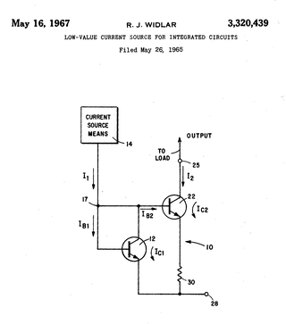
A Widlar current source is a modification of the basic two-transistor current mirror that incorporates an emitter degeneration resistor for only the output transistor, enabling the current source to generate low currents using only moderate resistor values.

A capacitance multiplier is designed to make a capacitor function like a much larger capacitor. This can be achieved in at least two ways.

An avalanche transistor is a bipolar junction transistor designed for operation in the region of its collector-current/collector-to-emitter voltage characteristics beyond the collector-to-emitter breakdown voltage, called avalanche breakdown region. This region is characterized by avalanche breakdown, which is a phenomenon similar to Townsend discharge for gases, and negative differential resistance. Operation in the avalanche breakdown region is called avalanche-mode operation: it gives avalanche transistors the ability to switch very high currents with less than a nanosecond rise and fall times. Transistors not specifically designed for the purpose can have reasonably consistent avalanche properties; for example 82% of samples of the 15V high-speed switch 2N2369, manufactured over a 12-year period, were capable of generating avalanche breakdown pulses with rise time of 350 ps or less, using a 90V power supply as Jim Williams writes.

A phase-shift oscillator is a linear electronic oscillator circuit that produces a sine wave output. It consists of an inverting amplifier element such as a transistor or op amp with its output fed back to its input through a phase-shift network consisting of resistors and capacitors in a ladder network. The feedback network 'shifts' the phase of the amplifier output by 180 degrees at the oscillation frequency to give positive feedback. Phase-shift oscillators are often used at audio frequency as audio oscillators.

A Wilson current mirror is a three-terminal circuit that accepts an input current at the input terminal and provides a "mirrored" current source or sink output at the output terminal. The mirrored current is a precise copy of the input current. It may be used as a Wilson current source by applying a constant bias current to the input branch as in Fig. 2. The circuit is named after George R. Wilson, an integrated circuit design engineer who worked for Tektronix. Wilson devised this configuration in 1967 when he and Barrie Gilbert challenged each other to find an improved current mirror overnight that would use only three transistors. Wilson won the challenge.

A switched capacitor (SC) is an electronic circuit that implements a function by moving charges into and out of capacitors when electronic switches are opened and closed. Usually, non-overlapping clock signals are used to control the switches, so that not all switches are closed simultaneously. Filters implemented with these elements are termed switched-capacitor filters, which depend only on the ratios between capacitances and the switching frequency, and not on precise resistors. This makes them much more suitable for use within integrated circuits, where accurately specified resistors and capacitors are not economical to construct, but accurate clocks and accurate relative ratios of capacitances are economical.

<span class="mw-page-title-main">Bipolar transistor biasing</span> Process necessary for BJT amplifiers to work correctly

Bipolar transistors must be properly biased to operate correctly. In circuits made with individual devices, biasing networks consisting of resistors are commonly employed. Much more elaborate biasing arrangements are used in integrated circuits, for example, bandgap voltage references and current mirrors. The voltage divider configuration achieves the correct voltages by the use of resistors in certain patterns. By selecting the proper resistor values, stable current levels can be achieved that vary only little over temperature and with transistor properties such as β.

<span class="mw-page-title-main">Joule thief</span> Voltage booster electronic circuit

A joule thief is a minimalist self-oscillating voltage booster that is small, low-cost, and easy to build, typically used for driving small loads, such as driving an LED using a 1.5 volt battery. This circuit is also known by other names such as blocking oscillator, joule ringer, or vampire torch. It can use nearly all of the energy in a single-cell electric battery, even far below the voltage where other circuits consider the battery fully discharged ; hence the name, which suggests the notion that the circuit is stealing energy or "joules" from the source – the term is a pun on "jewel thief". The circuit is a variant of the blocking oscillator that forms an unregulated voltage boost converter.

A comparator is an electronic component that compares two input voltages. Comparators are closely related to operational amplifiers, but a comparator is designed to operate with positive feedback and with its output saturated at one power rail or the other. If necessary, an op-amp can be pressed into service as a poorly performing comparator, but its slew Rate will be impaired.

References

  1. Jain, R. P.; Anand, M. (1983). Digital Electronics Practice Using Integrated Circuits. Tata McGraw-Hill Education. p. 159. ISBN   0074516922.
  2. Rao, Prakash (2006). Pulse And Digital Circuits. Tata McGraw-Hill Education. p. 268. ISBN   0070606560.
  3. Clayton, G B (2013). Operational Amplifiers, 2nd Ed. Elsevier. p. 267. ISBN   978-1483135557.
  4. Abraham, H.; E. Bloch (1919). "Mesure en valeur absolue des périodes des oscillations électriques de haute fréquence" [Measurement of the periods of high frequency electrical oscillations]. Annales de Physique (in French). Paris: Société Française de Physique. 9 (1): 237–302. Bibcode:1919AnPh....9..237A. doi:10.1051/jphystap:019190090021100.
  5. Ginoux, Jean-Marc (2012). "Van der Pol and the history of relaxation oscillations: Toward the emergence of a concepts". Chaos: An Interdisciplinary Journal of Nonlinear Science. 22 (2): 023120. arXiv: 1408.4890 . Bibcode:2012Chaos..22b3120G. doi:10.1063/1.3670008. PMID   22757527. S2CID   293369.
  6. Multivibrator in IEEE Std. 100 Dictionary of Standards Terms 7th ed., IEEE Press, 2000 ISBN   0-7381-2601-2 page 718
  7. William Henry Eccles and Frank Wilfred Jordan, "Improvements in ionic relays" British patent number: GB 148582 (filed: 21 June 1918; published: 5 August 1920).
  8. Wilfred Bennett Lewis (1942). Electrical counting: with special reference to counting alpha and beta particles. CUP Archive. p. 68.
  9. The Electrician. 128. Feb 13, 1942.{{cite journal}}: Missing or empty |title= (help)
  10. Owen Standige Puckle and E. B. Moullin (1943). Time bases (scanning generators): their design and development, with notes on the cathode ray tube. Chapman & Hall Ltd. p. 51.
  11. Britton Chance (1949). Waveforms (Vol. 19 of MIT Radiation Lab Series ed.). McGraw-Hill Book Co. p.  167.
  12. O. S. Puckle (Jan 1949). "Development of Time Bases: The Principles of Known Circuits". Wireless Engineer. Iliffe Electrical Publications. 26 (1): 139.
  13. 1 2 Donald Fink (ed), Electronics Engineers' Handbook, McGraw Hill, 1975 ISBN   0-07-020980-4, page 16-40