Related Research Articles
A diode is a two-terminal electronic component that conducts current primarily in one direction. It has low resistance in one direction and high resistance in the other.

Electronics is a scientific and engineering discipline that studies and applies the principles of physics to design, create, and operate devices that manipulate electrons and other electrically charged particles. Electronics is a subfield of electrical engineering, but it differs from it in that it focuses on using active devices such as transistors, diodes, and integrated circuits to control and amplify the flow of electric current and to convert it from one form to another, such as from alternating current (AC) to direct current (DC) or from analog to digital. Electronics also encompasses the fields of microelectronics, nanoelectronics, optoelectronics, and quantum electronics, which deal with the fabrication and application of electronic devices at microscopic, nanoscopic, optical, and quantum scales.

An amplifier, electronic amplifier or (informally) amp is an electronic device that can increase the magnitude of a signal. It is a two-port electronic circuit that uses electric power from a power supply to increase the amplitude of a signal applied to its input terminals, producing a proportionally greater amplitude signal at its output. The amount of amplification provided by an amplifier is measured by its gain: the ratio of output voltage, current, or power to input. An amplifier is defined as a circuit that has a power gain greater than one.
A semiconductor is a material that has an electrical conductivity value falling between that of a conductor, such as copper, and an insulator, such as glass. Its resistivity falls as its temperature rises; metals behave in the opposite way. Its conducting properties may be altered in useful ways by introducing impurities ("doping") into the crystal structure. When two differently doped regions exist in the same crystal, a semiconductor junction is created. The behavior of charge carriers, which include electrons, ions, and electron holes, at these junctions is the basis of diodes, transistors, and most modern electronics. Some examples of semiconductors are silicon, germanium, gallium arsenide, and elements near the so-called "metalloid staircase" on the periodic table. After silicon, gallium arsenide is the second-most common semiconductor and is used in laser diodes, solar cells, microwave-frequency integrated circuits, and others. Silicon is a critical element for fabricating most electronic circuits.

A transistor is a semiconductor device used to amplify or switch electrical signals and power. It is one of the basic building blocks of modern electronics. It is composed of semiconductor material, usually with at least three terminals for connection to an electronic circuit. A voltage or current applied to one pair of the transistor's terminals controls the current through another pair of terminals. Because the controlled (output) power can be higher than the controlling (input) power, a transistor can amplify a signal. Some transistors are packaged individually, but many more in miniature form are found embedded in integrated circuits. Because transistors are the key active components in practically all modern electronics, many people consider them one of the 20th century's greatest inventions.

A semiconductor device is an electronic component that relies on the electronic properties of a semiconductor material for its function. Its conductivity lies between conductors and insulators. Semiconductor devices have replaced vacuum tubes in most applications. They conduct electric current in the solid state, rather than as free electrons across a vacuum or as free electrons and ions through an ionized gas.

The metal–oxide–semiconductor field-effect transistor is a type of field-effect transistor (FET), most commonly fabricated by the controlled oxidation of silicon. It has an insulated gate, the voltage of which determines the conductivity of the device. This ability to change conductivity with the amount of applied voltage can be used for amplifying or switching electronic signals. The term metal–insulator–semiconductor field-effect transistor (MISFET) is almost synonymous with MOSFET. Another near-synonym is insulated-gate field-effect transistor (IGFET).
An insulated-gate bipolar transistor (IGBT) is a three-terminal power semiconductor device primarily forming an electronic switch. It was developed to combine high efficiency with fast switching. It consists of four alternating layers (P–N–P–N) that are controlled by a metal–oxide–semiconductor (MOS) gate structure.
This is an index of articles relating to electronics and electricity or natural electricity and things that run on electricity and things that use or conduct electricity.

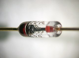
A tunnel diode or Esaki diode is a type of semiconductor diode that has effectively "negative resistance" due to the quantum mechanical effect called tunneling. It was invented in August 1957 by Leo Esaki when working at Tokyo Tsushin Kogyo, now known as Sony. In 1973, Esaki received the Nobel Prize in Physics for experimental demonstration of the electron tunneling effect in semiconductors. Robert Noyce independently devised the idea of a tunnel diode while working for William Shockley, but was discouraged from pursuing it. Tunnel diodes were first manufactured by Sony in 1957, followed by General Electric and other companies from about 1960, and are still made in low volume today.
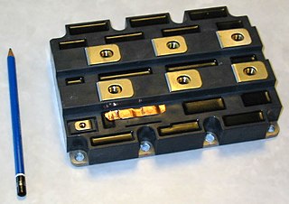
A power semiconductor device is a semiconductor device used as a switch or rectifier in power electronics. Such a device is also called a power device or, when used in an integrated circuit, a power IC.

A high-electron-mobility transistor, also known as heterostructure FET (HFET) or modulation-doped FET (MODFET), is a field-effect transistor incorporating a junction between two materials with different band gaps as the channel instead of a doped region. A commonly used material combination is GaAs with AlGaAs, though there is wide variation, dependent on the application of the device. Devices incorporating more indium generally show better high-frequency performance, while in recent years, gallium nitride HEMTs have attracted attention due to their high-power performance. Like other FETs, HEMTs are used in integrated circuits as digital on-off switches. FETs can also be used as amplifiers for large amounts of current using a small voltage as a control signal. Both of these uses are made possible by the FET’s unique current–voltage characteristics. HEMT transistors are able to operate at higher frequencies than ordinary transistors, up to millimeter wave frequencies, and are used in high-frequency products such as cell phones, satellite television receivers, voltage converters, and radar equipment. They are widely used in satellite receivers, in low power amplifiers and in the defense industry.
In computer engineering, a logic family is one of two related concepts:

An electronic component is any basic discrete electronic device or physical entity part of an electronic system used to affect electrons or their associated fields. Electronic components are mostly industrial products, available in a singular form and are not to be confused with electrical elements, which are conceptual abstractions representing idealized electronic components and elements. A datasheet for an electronic component is a technical document that provides detailed information about the component's specifications, characteristics, and performance.
A power MOSFET is a specific type of metal–oxide–semiconductor field-effect transistor (MOSFET) designed to handle significant power levels. Compared to the other power semiconductor devices, such as an insulated-gate bipolar transistor (IGBT) or a thyristor, its main advantages are high switching speed and good efficiency at low voltages. It shares with the IGBT an isolated gate that makes it easy to drive. They can be subject to low gain, sometimes to a degree that the gate voltage needs to be higher than the voltage under control.
In mesoscopic physics, ballistic conduction is the unimpeded flow of charge carriers, or energy-carrying particles, over relatively long distances in a material. In general, the resistivity of a material exists because an electron, while moving inside a medium, is scattered by impurities, defects, thermal fluctuations of ions in a crystalline solid, or, generally, by any freely-moving atom/molecule composing a gas or liquid. Without scattering, electrons simply obey Newton's second law of motion at non-relativistic speeds.
Hot carrier injection (HCI) is a phenomenon in solid-state electronic devices where an electron or a “hole” gains sufficient kinetic energy to overcome a potential barrier necessary to break an interface state. The term "hot" refers to the effective temperature used to model carrier density, not to the overall temperature of the device. Since the charge carriers can become trapped in the gate dielectric of a MOS transistor, the switching characteristics of the transistor can be permanently changed. Hot-carrier injection is one of the mechanisms that adversely affects the reliability of semiconductors of solid-state devices.
A transistor is a semiconductor device with at least three terminals for connection to an electric circuit. In the common case, the third terminal controls the flow of current between the other two terminals. This can be used for amplification, as in the case of a radio receiver, or for rapid switching, as in the case of digital circuits. The transistor replaced the vacuum-tube triode, also called a (thermionic) valve, which was much larger in size and used significantly more power to operate. The first transistor was successfully demonstrated on December 23, 1947, at Bell Laboratories in Murray Hill, New Jersey. Bell Labs was the research arm of American Telephone and Telegraph (AT&T). The three individuals credited with the invention of the transistor were William Shockley, John Bardeen and Walter Brattain. The introduction of the transistor is often considered one of the most important inventions in history.

The field-effect transistor (FET) is a type of transistor that uses an electric field to control the flow of current in a semiconductor. It comes in two types: junction-gate FET (JFET) and metal-oxide-semiconductor FET (MOSFET). FETs have three terminals: source, gate, and drain. FETs control the flow of current by the application of a voltage to the gate, which in turn alters the conductivity between the drain and source.
References
- ↑ Quentin Diduck; Martin Margala; Marc J. Feldman (20 November 2006). "A Terahertz Transistor Based on Geometrical Deflection of Ballistic Current". 2006 IEEE MTT-S International Microwave Symposium Digest. pp. 345–347. doi:10.1109/MWSYM.2006.249522. ISBN 978-0-7803-9541-1. S2CID 8542845.
- 1 2 3 4 Sherwood, Jonathan. "Radical 'Ballistic Computing' Chip Bounces Electrons Like Billards". Archived from the original on 24 February 2013. Retrieved 17 August 2006.
- 1 2 3 4 5 6 Bell, Trudy E. (February 1986). "The Quest for Ballistic Action". IEEE Spectrum. 2. 23 (2): 36–38. Bibcode:1986IEEES..23...36B. doi:10.1109/mspec.1986.6370997. S2CID 36115685.
- 1 2 Natori, Kenji (6 July 1994). "Ballistic metal-oxide semiconductor field effect transistor". Journal of Applied Physics. 76 (8): 4879–4890. Bibcode:1994JAP....76.4879N. doi:10.1063/1.357263. hdl: 2241/88704 .
- ↑ Dyakonov, Michael; Michael Shur (11 October 1993). "Shallow Water Analogy for a Ballistic Field Effect Transistor: New Mechanism of Plasma Wave Generation by dc Current". Physical Review Letters. 71 (15): 2465–2468. Bibcode:1993PhRvL..71.2465D. doi:10.1103/PhysRevLett.71.2465. PMID 10054687.