A logic gate is a device that performs a Boolean function, a logical operation performed on one or more binary inputs that produces a single binary output. Depending on the context, the term may refer to an ideal logic gate, one that has, for instance, zero rise time and unlimited fan-out, or it may refer to a non-ideal physical device[1] (see ideal and real op-amps for comparison).
Logic gates can be cascaded in the same way that Boolean functions can be composed, allowing the construction of a physical model of all of Boolean logic, and therefore, all of the algorithms and mathematics that can be described with Boolean logic. Logic circuits include such devices as multiplexers, registers, arithmetic logic units (ALUs), and computer memory, all the way up through complete microprocessors,[5] which may contain more than 100 million logic gates.
Compound logic gates AND-OR-Invert (AOI) and OR-AND-Invert (OAI) are often employed in circuit design because their construction using MOSFETs is simpler and more efficient than the sum of the individual gates.[6]
From 1934 to 1936, NEC engineer Akira Nakashima, Claude Shannon and Victor Shestakov introduced switching circuit theory in a series of papers showing that two-valuedBoolean algebra, which they discovered independently, can describe the operation of switching circuits.[10][11][12][13] Using this property of electrical switches to implement logic is the fundamental concept that underlies all electronic digital computers. Switching circuit theory became the foundation of digital circuit design, as it became widely known in the electrical engineering community during and after World War II, with theoretical rigor superseding the ad hoc methods that had prevailed previously.[13]
A synchronous 4-bit up/down decade counter symbol (74LS192) in accordance with ANSI/IEEE Std. 91-1984 and IEC Publication 60617-12.
There are two sets of symbols for elementary logic gates in common use, both defined in ANSI/IEEE Std 91-1984 and its supplement ANSI/IEEE Std 91a-1991. The "distinctive shape" set, based on traditional schematics, is used for simple drawings and derives from United States Military Standard MIL-STD-806 of the 1950s and 1960s.[16] It is sometimes unofficially described as "military", reflecting its origin. The "rectangular shape" set, based on ANSI Y32.14 and other early industry standards as later refined by IEEE and IEC, has rectangular outlines for all types of gate and allows representation of a much wider range of devices than is possible with the traditional symbols.[17] The IEC standard, IEC 60617-12, has been adopted by other standards, such as EN 60617-12:1999 in Europe, BS EN 60617-12:1999 in the United Kingdom, and DIN EN 60617-12:1998 in Germany.
The mutual goal of IEEE Std 91-1984 and IEC 617-12 was to provide a uniform method of describing the complex logic functions of digital circuits with schematic symbols. These functions were more complex than simple AND and OR gates. They could be medium-scale circuits such as a 4-bit counter to a large-scale circuit such as a microprocessor.
IEC 617-12 and its renumbered successor IEC 60617-12 do not explicitly show the "distinctive shape" symbols, but do not prohibit them.[17] These are, however, shown in ANSI/IEEE Std 91 (and 91a) with this note: "The distinctive-shape symbol is, according to IEC Publication 617, Part 12, not preferred, but is not considered to be in contradiction to that standard." IEC 60617-12 correspondingly contains the note (Section 2.1) "Although non-preferred, the use of other symbols recognized by official national standards, that is distinctive shapes in place of symbols [list of basic gates], shall not be considered to be in contradiction with this standard. Usage of these other symbols in combination to form complex symbols (for example, use as embedded symbols) is discouraged." This compromise was reached between the respective IEEE and IEC working groups to permit the IEEE and IEC standards to be in mutual compliance with one another.
In electronics a NOT gate is more commonly called an inverter. The circle on the symbol is called a bubble and is used in logic diagrams to indicate a logic negation between the external logic state and the internal logic state (1 to 0 or vice versa). On a circuit diagram it must be accompanied by a statement asserting that the positive logic convention or negative logic convention is being used (high voltage level = 1 or low voltage level = 1, respectively). The wedge is used in circuit diagrams to directly indicate an active-low (low voltage level = 1) input or output without requiring a uniform convention throughout the circuit diagram. This is called Direct Polarity Indication. See IEEE Std 91/91A and IEC 60617-12. Both the bubble and the wedge can be used on distinctive-shape and rectangular-shape symbols on circuit diagrams, depending on the logic convention used. On pure logic diagrams, only the bubble is meaningful.
The output of a two input exclusive-OR is true only when the two input values are different, and false if they are equal, regardless of the value. If there are more than two inputs, the output of the distinctive-shape symbol is undefined. The output of the rectangular-shaped symbol is true if the number of true inputs is exactly one or exactly the number following the "=" in the qualifying symbol.
By use of De Morgan's laws, an AND function is identical to an OR function with negated inputs and outputs. Likewise, an OR function is identical to an AND function with negated inputs and outputs. A NAND gate is equivalent to an OR gate with negated inputs, and a NOR gate is equivalent to an AND gate with negated inputs.
This leads to an alternative set of symbols for basic gates that use the opposite core symbol (AND or OR) but with the inputs and outputs negated. Use of these alternative symbols can make logic circuit diagrams much clearer and help to show accidental connection of an active high output to an active low input or vice versa. Any connection that has logic negations at both ends can be replaced by a negationless connection and a suitable change of gate or vice versa. Any connection that has a negation at one end and no negation at the other can be made easier to interpret by instead using the De Morgan equivalent symbol at either of the two ends. When negation or polarity indicators on both ends of a connection match, there is no logic negation in that path (effectively, bubbles "cancel"), making it easier to follow logic states from one symbol to the next. This is commonly seen in real logic diagrams – thus the reader must not get into the habit of associating the shapes exclusively as OR or AND shapes, but also take into account the bubbles at both inputs and outputs in order to determine the "true" logic function indicated.
A De Morgan symbol can show more clearly a gate's primary logical purpose and the polarity of its nodes that are considered in the "signaled" (active, on) state. Consider the simplified case where a two-input NAND gate is used to drive a motor when either of its inputs are brought low by a switch. The "signaled" state (motor on) occurs when either one OR the other switch is on. Unlike a regular NAND symbol, which suggests AND logic, the De Morgan version, a two negative-input OR gate, correctly shows that OR is of interest. The regular NAND symbol has a bubble at the output and none at the inputs (the opposite of the states that will turn the motor on), but the De Morgan symbol shows both inputs and output in the polarity that will drive the motor.
De Morgan's theorem is most commonly used to implement logic gates as combinations of only NAND gates, or as combinations of only NOR gates, for economic reasons.
Charles Sanders Peirce (during 1880–1881) showed that NOR gates alone (or alternatively NAND gates alone) can be used to reproduce the functions of all the other logic gates, but his work on it was unpublished until 1933.[18] The first published proof was by Henry M. Sheffer in 1913, so the NAND logical operation is sometimes called Sheffer stroke; the logical NOR is sometimes called Peirce's arrow.[19] Consequently, these gates are sometimes called universal logic gates.[20]
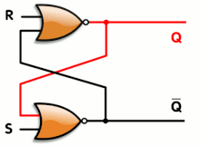
Logic gates can also be used to hold a state, allowing data storage. A storage element can be constructed by connecting several gates in a "latch" circuit. Latching circuitry is used in static random-access memory. More complicated designs that use clock signals and that change only on a rising or falling edge of the clock are called edge-triggered "flip-flops". Formally, a flip-flop is called a bistable circuit, because it has two stable states which it can maintain indefinitely. The combination of multiple flip-flops in parallel, to store a multiple-bit value, is known as a register. When using any of these gate setups the overall system has memory; it is then called a sequential logic system since its output can be influenced by its previous state(s), i.e. by the sequence of input states. In contrast, the output from combinational logic is purely a combination of its present inputs, unaffected by the previous input and output states.
These logic circuits are used in computer memory. They vary in performance, based on factors of speed, complexity, and reliability of storage, and many different types of designs are used based on the application.
Electronic logic gates differ significantly from their relay-and-switch equivalents. They are much faster, consume much less power, and are much smaller (all by a factor of a million or more in most cases). Also, there is a fundamental structural difference. The switch circuit creates a continuous metallic path for current to flow (in either direction) between its input and its output. The semiconductor logic gate, on the other hand, acts as a high-gainvoltageamplifier, which sinks a tiny current at its input and produces a low-impedance voltage at its output. It is not possible for current to flow between the output and the input of a semiconductor logic gate.
The 7400 chip, containing four NANDs. The two additional pins supply power (+5 V) and connect the ground.
For small-scale logic, designers now use prefabricated logic gates from families of devices such as the TTL7400 series by Texas Instruments, the CMOS4000 series by RCA, and their more recent descendants. Increasingly, these fixed-function logic gates are being replaced by programmable logic devices, which allow designers to pack many mixed logic gates into a single integrated circuit. The field-programmable nature of programmable logic devices such as FPGAs has reduced the 'hard' property of hardware; it is now possible to change the logic design of a hardware system by reprogramming some of its components, thus allowing the features or function of a hardware implementation of a logic system to be changed.
An important advantage of standardized integrated circuit logic families, such as the 7400 and 4000 families, is that they can be cascaded. This means that the output of one gate can be wired to the inputs of one or several other gates, and so on. Systems with varying degrees of complexity can be built without great concern of the designer for the internal workings of the gates, provided the limitations of each integrated circuit are considered.
The output of one gate can only drive a finite number of inputs to other gates, a number called the 'fan-out limit'. Also, there is always a delay, called the 'propagation delay', from a change in input of a gate to the corresponding change in its output. When gates are cascaded, the total propagation delay is approximately the sum of the individual delays, an effect which can become a problem in high-speed synchronous circuits. Additional delay can be caused when many inputs are connected to an output, due to the distributed capacitance of all the inputs and wiring and the finite amount of current that each output can provide.
There are several logic families with different characteristics (power consumption, speed, cost, size) such as: RDL (resistor–diode logic), RTL (resistor-transistor logic), DTL (diode–transistor logic), TTL (transistor–transistor logic) and CMOS. There are also sub-variants, e.g. standard CMOS logic vs. advanced types using still CMOS technology, but with some optimizations for avoiding loss of speed due to slower PMOS transistors.
The simplest family of logic gates uses bipolar transistors, and is called resistor–transistor logic (RTL). Unlike simple diode logic gates (which do not have a gain element), RTL gates can be cascaded indefinitely to produce more complex logic functions. RTL gates were used in early integrated circuits. For higher speed and better density, the resistors used in RTL were replaced by diodes resulting in diode–transistor logic (DTL). Transistor–transistor logic (TTL) then supplanted DTL.
CMOS diagram of a NOT gate, also known as an inverter. MOSFETs are the most common way to make logic gates.
As integrated circuits became more complex, bipolar transistors were replaced with smaller field-effect transistors (MOSFETs); see PMOS and NMOS. To reduce power consumption still further, most contemporary chip implementations of digital systems now use CMOS logic. CMOS uses complementary (both n-channel and p-channel) MOSFET devices to achieve a high speed with low power dissipation.
Other types of logic gates include, but are not limited to:[21]
Uses transistors switching between saturated and cutoff states to perform logic. The transistors require carefully controlled parameters. Economical because few other components are needed, but tends to be susceptible to noise because of the lower voltage levels employed. Often considered to be the father to modern TTL logic.
Uses MOSFETs (metal–oxide–semiconductor field-effect transistors), the basis for most modern logic gates. The MOS logic family includes PMOS logic, NMOS logic, complementary MOS (CMOS), and BiCMOS (bipolar CMOS).
Uses transistors to perform logic but biasing is from constant current sources to prevent saturation and allow extremely fast switching. Has high noise immunity despite fairly low logic levels.
Uses tunnelable q-bits for synthesizing the binary logic bits. The electrostatic repulsive force in between two electrons in the quantum dots assigns the electron configurations (that defines state 1 or state 0) under the suitably driven polarizations. This is a transistorless, currentless, junctionless binary logic synthesis technique allowing it to have very fast operation speeds.
Ferroelectric FET
FeFET
FeFET transistors can retain their state to speed recovery in case of a power loss.[22]
Three-state logic gates
A tristate buffer can be thought of as a switch. If B is on, the switch is closed. If B is off, the switch is open.
A three-state logic gate is a type of logic gate that can have three different outputs: high (H), low (L) and high-impedance (Z). The high-impedance state plays no role in the logic, which is strictly binary. These devices are used on buses of the CPU to allow multiple chips to send data. A group of three-states driving a line with a suitable control circuit is basically equivalent to a multiplexer, which may be physically distributed over separate devices or plug-in cards.
In electronics, a high output would mean the output is sourcing current from the positive power terminal (positive voltage). A low output would mean the output is sinking current to the negative power terminal (zero voltage). High impedance would mean that the output is effectively disconnected from the circuit.
Non-electronic logic gates
Non-electronic implementations are varied, though few of them are used in practical applications. Many early electromechanical digital computers, such as the Harvard Mark I, were built from relay logic gates, using electro-mechanical relays. Logic gates can be made using pneumatic devices, such as the Sorteberg relay or mechanical logic gates, including on a molecular scale.[23] Various types of fundamental logic gates have been constructed using molecules (molecular logic gates), which are based on chemical inputs and spectroscopic outputs.[24] Logic gates have been made out of DNA (see DNA nanotechnology)[25] and used to create a computer called MAYA (see MAYA-II). Logic gates can be made from quantum mechanical effects, see quantum logic gate. Photonic logic gates use nonlinear optical effects.
In principle any method that leads to a gate that is functionally complete (for example, either a NOR or a NAND gate) can be used to make any kind of digital logic circuit. Note that the use of 3-state logic for bus systems is not needed, and can be replaced by digital multiplexers, which can be built using only simple logic gates (such as NAND gates, NOR gates, or AND and OR gates).
Digital electronics is a field of electronics involving the study of digital signals and the engineering of devices that use or produce them. This is in contrast to analog electronics which work primarily with analog signals. Despite the name, digital electronics designs includes important analog design considerations.
Transistor–transistor logic (TTL) is a logic family built from bipolar junction transistors. Its name signifies that transistors perform both the logic function and the amplifying function, as opposed to earlier resistor–transistor logic (RTL) and diode–transistor logic (DTL).
NMOS or nMOS logic uses n-type (-) MOSFETs to implement logic gates and other digital circuits.
Complementary metal–oxide–semiconductor is a type of metal–oxide–semiconductor field-effect transistor (MOSFET) fabrication process that uses complementary and symmetrical pairs of p-type and n-type MOSFETs for logic functions. CMOS technology is used for constructing integrated circuit (IC) chips, including microprocessors, microcontrollers, memory chips, and other digital logic circuits. CMOS technology is also used for analog circuits such as image sensors, data converters, RF circuits, and highly integrated transceivers for many types of communication.
In digital logic, an inverter or NOT gate is a logic gate which implements logical negation. It outputs a bit opposite of the bit that is put into it. The bits are typically implemented as two differing voltage levels.
The 7400 series is a popular logic family of transistor–transistor logic (TTL) integrated circuits (ICs).
Resistor–transistor logic (RTL), sometimes also known as transistor–resistor logic (TRL), is a class of digital circuits built using resistors as the input network and bipolar junction transistors (BJTs) as switching devices. RTL is the earliest class of transistorized digital logic circuit; it was succeeded by diode–transistor logic (DTL) and transistor–transistor logic (TTL).
In computer engineering, a logic family is one of two related concepts:
The AND gate is a basic digital logic gate that implements logical conjunction (∧) from mathematical logic – AND gate behaves according to the truth table. A HIGH output (1) results only if all the inputs to the AND gate are HIGH (1). If not all inputs to the AND gate are HIGH, LOW output results. The function can be extended to any number of inputs.
The OR gate is a digital logic gate that implements logical disjunction. The OR gate outputs "true" if any of its inputs are "true"; otherwise it outputs "false". The input and output states are normally represented by different voltage levels.
In digital electronics, a NAND gate (NOT-AND) is a logic gate which produces an output which is false only if all its inputs are true; thus its output is complement to that of an AND gate. A LOW (0) output results only if all the inputs to the gate are HIGH (1); if any input is LOW (0), a HIGH (1) output results. A NAND gate is made using transistors and junction diodes. By De Morgan's laws, a two-input NAND gate's logic may be expressed as , making a NAND gate equivalent to inverters followed by an OR gate.
An electronic symbol is a pictogram used to represent various electrical and electronic devices or functions, such as wires, batteries, resistors, and transistors, in a schematic diagram of an electrical or electronic circuit. These symbols are largely standardized internationally today, but may vary from country to country, or engineering discipline, based on traditional conventions.
XOR gate is a digital logic gate that gives a true output when the number of true inputs is odd. An XOR gate implements an exclusive or from mathematical logic; that is, a true output results if one, and only one, of the inputs to the gate is true. If both inputs are false (0/LOW) or both are true, a false output results. XOR represents the inequality function, i.e., the output is true if the inputs are not alike otherwise the output is false. A way to remember XOR is "must have one or the other but not both".
The NAND Boolean function has the property of functional completeness. This means that any Boolean expression can be re-expressed by an equivalent expression utilizing only NAND operations. For example, the function NOT(x) may be equivalently expressed as NAND(x,x). In the field of digital electronic circuits, this implies that it is possible to implement any Boolean function using just NAND gates.
The XNOR gate is a digital logic gate whose function is the logical complement of the Exclusive OR (XOR) gate. It is equivalent to the logical connective from mathematical logic, also known as the material biconditional. The two-input version implements logical equality, behaving according to the truth table to the right, and hence the gate is sometimes called an "equivalence gate". A high output (1) results if both of the inputs to the gate are the same. If one but not both inputs are high (1), a low output (0) results.
The NOR gate is a digital logic gate that implements logical NOR - it behaves according to the truth table to the right. A HIGH output (1) results if both the inputs to the gate are LOW (0); if one or both input is HIGH (1), a LOW output (0) results. NOR is the result of the negation of the OR operator. It can also in some senses be seen as the inverse of an AND gate. NOR is a functionally complete operation—NOR gates can be combined to generate any other logical function. It shares this property with the NAND gate. By contrast, the OR operator is monotonic as it can only change LOW to HIGH but not vice versa.
Diode logic constructs AND and OR logic gates with diodes and resistors.
An electronic circuit is composed of individual electronic components, such as resistors, transistors, capacitors, inductors and diodes, connected by conductive wires or traces through which electric current can flow. It is a type of electrical circuit. For a circuit to be referred to as electronic, rather than electrical, generally at least one active component must be present. The combination of components and wires allows various simple and complex operations to be performed: signals can be amplified, computations can be performed, and data can be moved from one place to another.
A truth table is a mathematical table used in logic—specifically in connection with Boolean algebra, Boolean functions, and propositional calculus—which sets out the functional values of logical expressions on each of their functional arguments, that is, for each combination of values taken by their logical variables. In particular, truth tables can be used to show whether a propositional expression is true for all legitimate input values, that is, logically valid.
↑ Perkins, Franklin (2004). "Exchange with China". Leibniz and China: A Commerce of Light. Cambridge University Press. p.117. ISBN9780521830249. ... one of the traditional orderings of the hexagrams, the xiantian tu ordering made by Shao Yong, was, with a few modifications, the same order found in Leibniz's binary arithmetic.
This page is based on this Wikipedia article Text is available under the CC BY-SA 4.0 license; additional terms may apply. Images, videos and audio are available under their respective licenses.