This article's lead sectionmay be too short to adequately summarize the key points. Please consider expanding the lead to provide an accessible overview of all important aspects of the article.(January 2013)
A simplified PAL device. The programmable elements (shown as a fuse) connect both the true and complemented inputs to the AND gates. These AND gates, also known as product terms, are ORed together to form a sum-of-products logic array.
A programmable logic device (PLD) is an electronic component used to build reconfigurabledigital circuits. Unlike digital logic constructed using discrete logic gates with fixed functions, the function of a PLD is undefined at the time of manufacture. Before the PLD can be used in a circuit it must be programmed to implement the desired function.[1] Compared to fixed logic devices, programmable logic devices simplify the design of complex logic and may offer superior performance.[2] Unlike for microprocessors, programming a PLD changes the connections made between the gates in the device.
In 1969, Motorola offered the XC157, a mask-programmed gate array with 12 gates and 30 uncommitted input/output pins.[3]
In 1970, Texas Instruments developed a mask-programmable IC based on the IBM read-only associative memory or ROAM. This device, the TMS2000, was programmed by altering the metal layer during the production of the IC. The TMS2000 had up to 17 inputs and 18 outputs with 8 JK flip-flops for memory. TI coined the term Programmable Logic Array (PLA) for this device.[4]
In 1971, General Electric Company (GE) was developing a programmable logic device based on the new Programmable Read-Only Memory (PROM) technology. This experimental device improved on IBM's ROAM by allowing multilevel logic. Intel had just introduced the floating-gate UVerasable PROM so the researcher at GE incorporated that technology. The GE device was the first erasable PLD ever developed, predating the Altera EPLD by over a decade. GE obtained several early patents on programmable logic devices.[5][6][7]
In 1973 National Semiconductor introduced a mask-programmable PLA device (DM7575) with 14 inputs and 8 outputs with no memory registers. This was more popular than the TI part but the cost of making the metal mask limited its use. The device is significant because it was the basis for the field programmable logic array produced by Signetics in 1975, the 82S100. (Intersil actually beat Signetics to market but poor yield doomed their part.)[8][9]
In 1974 GE entered into an agreement with Monolithic Memories (MMI) to develop a mask-programmable logic device incorporating the GE innovations. The device was named the 'Programmable Associative Logic Array' or PALA. The MMI 5760 was completed in 1976 and could implement multilevel or sequential circuits of over 100 gates. The device was supported by a GE design environment where Boolean equations would be converted to mask patterns for configuring the device. The part was never brought to market.[10]
In 1970, Texas Instruments developed a mask-programmable IC based on the IBM read-only associative memory or ROAM. This device, the TMS2000, was programmed by altering the metal layer during the production of the IC. The TMS2000 had up to 17 inputs and 18 outputs with 8 JK flip-flops for memory. TI coined the term programmable logic array for this device.[4]
A programmable logic array (PLA) has a programmable AND gate array, which links to a programmable OR gate array, which can then be conditionally complemented to produce an output. A PLA is similar to a ROM concept, however a PLA does not provide full decoding of a variable and does not generate all the minterms as in a ROM.
PAL devices have arrays of transistor cells arranged in a "fixed-OR, programmable-AND" plane used to implement "sum-of-products" binary logic equations for each of the outputs in terms of the inputs and either synchronous or asynchronous feedback from the outputs.
MMI introduced a breakthrough device in 1978, the programmable array logic or PAL. The architecture was simpler than that of Signetics' FPLA because it omitted the programmable OR array. This made the parts faster, smaller and cheaper. They were available in 20-pin 300-mil DIP packages, while the FPLAs came in 28-pin 600-mil packages. The PAL Handbook demystified the design process. The PALASM design software (PAL assembler) converted the engineers' Boolean equations into the fuse pattern required to program the part. The PAL devices were soon second-sourced by National Semiconductor, Texas Instruments and AMD.
After MMI succeeded with the 20-pin PAL parts, AMD introduced the 24-pin 22V10 PAL with additional features. After buying out MMI (1987), AMD spun off a consolidated operation as Vantis, and that business was acquired by Lattice Semiconductor in 1999.
An improvement on the PAL was the generic array logic device, or GAL, invented by Lattice Semiconductor in 1985. This device has the same logical properties as the PAL but can be erased and reprogrammed. The GAL is very useful in the prototyping stage of a design, when any bugs in the logic can be corrected by reprogramming. GALs are programmed and reprogrammed using a PAL programmer, or, in the case of chips that support it, by using the in-circuit programming technique.
Lattice GALs combine CMOS and electrically erasable (E2) floating gate technology for a high-speed, low-power logic device. A similar device called a PEEL (programmable electrically erasable logic) was introduced by the International CMOS Technology (ICT) corporation.
PALs and GALs are available only in small sizes, equivalent to a few hundred logic gates. For bigger logic circuits, complex PLDs or CPLDs can be used. These contain the equivalent of several PALs linked by programmable interconnections, all in one integrated circuit. CPLDs can replace thousands, or even hundreds of thousands, of logic gates.
Some CPLDs are programmed using a PAL programmer, but this method becomes inconvenient for devices with hundreds of pins. A second method of programming is to solder the device to its printed circuit board, then feed it with a serial data stream from a personal computer. The CPLD contains a circuit that decodes the data stream and configures the CPLD to perform its specified logic function. Some manufacturers (including Altera and Microsemi) use JTAG to program CPLDs in-circuit from .JAM files.
While PALs were being developed into GALs and CPLDs (all discussed above), a separate stream of development was happening. This type of device is based on gate array technology and is called the field-programmable gate array (FPGA). Early examples of FPGAs are the 82S100 array, and 82S105 sequencer, by Signetics, introduced in the late 1970s. The 82S100 was an array of AND terms. The 82S105 also had flip-flop functions.
(Remark: 82S100 and similar ICs from Signetics have PLA structure, AND-plane + OR-plane.)
FPGAs use a grid of logic gates, and once stored, the data doesn't change, similar to that of an ordinary gate array. The term field-programmable means the device is programmed by the customer, not the manufacturer. FPGAs and gate arrays are similar but gate arrays can only be configured at the factory during fabrication.[11][12][13]
FPGAs are usually programmed after being soldered down to the circuit board, in a manner similar to that of larger CPLDs. In most larger FPGAs, the configuration is volatile and must be re-loaded into the device whenever power is applied or different functionality is required. Configuration is typically stored in a configuration PROM, EEPROM or flash memory.[14] EEPROM versions may be in-system programmable (typically via JTAG).
The difference between FPGAs and CPLDs is that FPGAs are internally based on look-up tables (LUTs), whereas CPLDs form the logic functions with sea-of-gates (e.g. sum of products). CPLDs are meant for simpler designs while FPGAs are meant for more complex designs. In general, CPLDs are a good choice for wide combinational logic applications, whereas FPGAs are more suitable for large state machines such as microprocessors.
Using the same technology as EPROMs, EPLDs have a quartz window in the package that allows them to be erased on exposure to UV light.[15][16]
Using the same technology as EEPROMs, EEPLDs can be erased electrically.[15][16]
An Erasable programmable logic device (EPLD) is an integrated circuit that comprises an array of PLDs that do not come pre-connected; the connections are programmed electrically by the user. Most GAL and FPGA devices are examples of EPLDs. [citation needed]
Other variants
These are microprocessor circuits that contain some fixed functions and other functions that can be altered by code running on the processor. Designing self-altering systems requires that engineers learn new methods, and that new software tools be developed.
PLDs are being sold now that contain a microprocessor with a fixed function (the so-called core) surrounded by programmable logic. These devices let designers concentrate on adding new features to designs without having to worry about making the microprocessor work. Also, the fixed-function microprocessor takes less space on the chip than a part of the programmable gate array implementing the same processor, leaving more space for the programmable gate array to contain the designer's specialized circuits.
How PLDs retain their configuration
A PLD is a combination of a logic device and a memory device. The memory is used to store the pattern that was given to the chip during programming. Most of the methods for storing data in an integrated circuit have been adapted for use in PLDs. These include:
Silicon antifuses are connections that are made by applying a voltage across a modified area of silicon inside the chip. They are called antifuses because they work in the opposite way to normal fuses, which begin life as connections until they are broken by an electric current.
SRAM, or static RAM, is a volatile type of memory, meaning that its contents are lost each time the power is switched off. SRAM-based PLDs therefore have to be programmed every time the circuit is switched on. This is usually done automatically by another part of the circuit.
An EPROM memory cell is a MOSFET (metal-oxide semiconductor field-effect transistor, or MOS transistor) that can be switched on by trapping an electric charge permanently on its gate electrode. This is done by a PAL programmer. The charge remains for many years and can only be removed by exposing the chip to strong ultraviolet light in a device called an EPROM eraser.
Flash memory is non-volatile, retaining its contents even when the power is switched off. It is stored on floating-gate MOSFET memory cells, and can be erased and reprogrammed as required. This makes it useful in PLDs that may be reprogrammed frequently, such as PLDs used in prototypes. Flash memory is a kind of EEPROM that holds information using trapped electric charges similar to EPROM. Consequently, flash memory can hold information for years, but possibly not as many years as EPROM.
As of 2005, most CPLDs are electrically programmable and erasable, and non-volatile. This is because they are too small to justify the inconvenience of programming internal SRAM cells every time they start up, and EPROM cells are more expensive due to their ceramic package with a quartz window.
PALASM, ABEL and CUPL are frequently used for low-complexity devices, while Verilog and VHDL are popular higher-level description languages for more complex devices. The more limited ABEL is often used for historical reasons, but for new designs VHDL is more popular, even for low-complexity designs.
A device programmer is used to transfer the boolean logic pattern into the programmable device. In the early days of programmable logic, every PLD manufacturer also produced a specialized device programmer for its family of logic devices. Later, universal device programmers came onto the market that supported several logic device families from different manufacturers. Today's device programmers usually can program common PLDs (mostly PAL/GAL equivalents) from all existing manufacturers. Common file formats used to store the boolean logic pattern (fuses) are JEDEC, Altera POF (programmable object file), or Xilinx BITstream.[17]
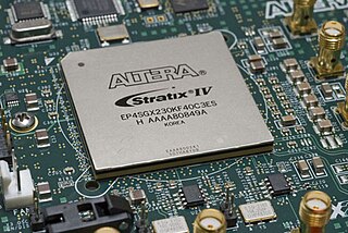
A field-programmable gate array (FPGA) is a type of configurable integrated circuit that can be programmed or reprogrammed after manufacturing. FPGAs are part of a broader set of logic devices referred to as programmable logic devices (PLDs). They consist of an array of programmable logic blocks and interconnects that can be configured to perform various digital functions. FPGAs are commonly used in applications where flexibility, speed, and parallel processing capabilities are required, such as in telecommunications, automotive, aerospace, and industrial sectors.
A logic gate is a device that performs a Boolean function, a logical operation performed on one or more binary inputs that produces a single binary output. Depending on the context, the term may refer to an ideal logic gate, one that has, for instance, zero rise time and unlimited fan-out, or it may refer to a non-ideal physical device.
A microcontroller or microcontroller unit (MCU) is a small computer on a single integrated circuit. A microcontroller contains one or more CPUs along with memory and programmable input/output peripherals. Program memory in the form of ferroelectric RAM, NOR flash or OTP ROM is also often included on chip, as well as a small amount of RAM. Microcontrollers are designed for embedded applications, in contrast to the microprocessors used in personal computers or other general purpose applications consisting of various discrete chips.
A programmable read-only memory (PROM) is a form of digital memory where the contents can be changed once after manufacture of the device. The data is then permanent and cannot be changed. It is one type of read-only memory (ROM). PROMs are used in digital electronic devices to store permanent data, usually low level programs such as firmware or microcode. The key difference from a standard ROM is that the data is written into a ROM during manufacture, while with a PROM the data is programmed into them after manufacture. Thus, ROMs tend to be used only for large production runs with well-verified data. PROMs may be used where the volume required does not make a factory-programmed ROM economical, or during development of a system that may ultimately be converted to ROMs in a mass produced version.
EEPROM or E2PROM (electrically erasable programmable read-only memory) is a type of non-volatile memory. It is used in computers, usually integrated in microcontrollers such as smart cards and remote keyless systems, or as a separate chip device, to store relatively small amounts of data by allowing individual bytes to be erased and reprogrammed.
An EPROM, or erasable programmable read-only memory, is a type of programmable read-only memory (PROM) chip that retains its data when its power supply is switched off. Computer memory that can retrieve stored data after a power supply has been turned off and back on is called non-volatile. It is an array of floating-gate transistors individually programmed by an electronic device that supplies higher voltages than those normally used in digital circuits. Once programmed, an EPROM can be erased by exposing it to strong ultraviolet (UV) light source. EPROMs are easily recognizable by the transparent fused quartz window on the top of the package, through which the silicon chip is visible, and which permits exposure to ultraviolet light during erasing.
An application-specific integrated circuit is an integrated circuit (IC) chip customized for a particular use, rather than intended for general-purpose use, such as a chip designed to run in a digital voice recorder or a high-efficiency video codec. Application-specific standard product chips are intermediate between ASICs and industry standard integrated circuits like the 7400 series or the 4000 series. ASIC chips are typically fabricated using metal–oxide–semiconductor (MOS) technology, as MOS integrated circuit chips.
A programmable logic array (PLA) is a kind of programmable logic device used to implement combinational logic circuits. The PLA has a set of programmable AND gate planes, which link to a set of programmable OR gate planes, which can then be conditionally complemented to produce an output. It has 2N AND gates for N input variables, and for M outputs from the PLA, there should be M OR gates, each with programmable inputs from all of the AND gates. This layout allows for many logic functions to be synthesized in the sum of products canonical forms.
Programmable Array Logic (PAL) is a family of programmable logic device semiconductors used to implement logic functions in digital circuits that was introduced by Monolithic Memories, Inc. (MMI) in March 1978. MMI obtained a registered trademark on the term PAL for use in "Programmable Semiconductor Logic Circuits". The trademark is currently held by Lattice Semiconductor.
A gate array is an approach to the design and manufacture of application-specific integrated circuits (ASICs) using a prefabricated chip with components that are later interconnected into logic devices according to custom order by adding metal interconnect layers in the factory. It was popular during the upheaval in the semiconductor industry in the 1980s, and its usage declined by the end of the 1990s.
A programmer, device programmer, chip programmer, device burner, or PROM writer is a piece of electronic equipment that arranges written software or firmware to configure programmable non-volatile integrated circuits, called programmable devices. The target devices include PROM, EPROM, EEPROM, Flash memory, eMMC, MRAM, FeRAM, NVRAM, PLDs, PLAs, PALs, GALs, CPLDs, FPGAs, and microcontrollers.
A complex programmable logic device (CPLD) is a programmable logic device with complexity between that of PALs and FPGAs, and architectural features of both. The main building block of the CPLD is a macrocell, which contains logic implementing disjunctive normal form expressions and more specialized logic operations.
Signetics Corporation was an American electronics manufacturer specifically established to make integrated circuits. Founded in 1961, they went on to develop a number of early microprocessors and support chips, as well as the widely used 555 timer chip. The company was bought by Philips in 1975 and incorporated in Philips Semiconductors.
The Generic Array Logic device was an innovation of the PAL and was invented by Lattice Semiconductor. The GAL was an improvement on the PAL because one device type was able to take the place of many PAL device types or could even have functionality not covered by the original range of PAL devices. Its primary benefit, however, was that it was erasable and re-programmable, making prototyping and design changes easier for engineers.
Data I/O Corporation is a provider of manual and automated data programming and security provisioning systems for flash memory, microcontrollers, and logic devices. Founded in 1969 and incorporated in 1972, the company developed equipment that allowed electronic designers to program non-volatile semiconductor devices with data stored on punched cards or ASCII-encoded (eight-level) punched paper tape. These products were used for the design and manufacturing of systems used in industries such as IoT, medical development, and consumer electronics. Over the next three decades, the company was involved in technologies such as Bipolar, EPROM, EEPROM, NOR FLASH, Antifuse, FRAM, NAND FLASH, eMMC, and Universal Flash Storage (UFS) devices.
An electronic device or embedded system is said to be field-programmable or in-place programmable if its firmware can be modified "in the field", without disassembling the device or returning it to its manufacturer.
A simple programmable logic device (SPLD) is a programmable logic device with complexity below that of a complex programmable logic device (CPLD).
Read-only memory (ROM) is a type of non-volatile memory used in computers and other electronic devices. Data stored in ROM cannot be electronically modified after the manufacture of the memory device. Read-only memory is useful for storing software that is rarely changed during the life of the system, also known as firmware. Software applications for programmable devices can be distributed as plug-in cartridges containing ROM.
The following outline is provided as an overview of and topical guide to electronics:
The GAL22V10 is a series of programmable-logic devices from Lattice Semiconductor, implemented as CMOS-based generic array logic ICs, and available in dual inline packages or plastic leaded chip carriers. It is an example of a standard production GAL device that is often used in educational settings as a basic programmable-logic device. In combinatorial mode, it is conceptually a group of programmable AND-OR-invert (AOI) (AND-NOR) gates or AND-OR gates.
References
1 2 Horowitz, Paul; Hill, Winfield (2015). Horowitz P., Hill W. - The Art of Electronics. New York. p.764. ISBN978-0-521-80926-9.{{cite book}}: CS1 maint: location missing publisher (link)
↑ Motorola Semiconductor Data Book, Fourth Edition. Motorola Inc. 1969. p.IC-73.
1 2 Andres, Kent (October 1970). A Texas Instruments Application Report: MOS programmable logic arrays. Texas Instruments. Bulletin CA-158. Report introduces the TMS2000 and TMS2200 series of mask programmable PLAs.
↑ Greer, David L. Electrically Programmable Logic CircuitsUS Patent 3,818,452. Assignee: General Electric, Filed: April 28, 1972, Granted: June 18, 1974
↑ Greer, David L. Multiple Level Associative Logic CircuitsUS Patent 3,816,725. Assignee: General Electric, Filed: April 28, 1972, Granted: June 11, 1974
↑ Greer, David L. Segmented Associative Logic CircuitsUS Patent 3,849,638. Assignee: General Electric, Filed: July 18, 1973, Granted: November 19, 1974
↑ "Semiconductors and IC's: FPLA". EDN. 20 (13). Boston, MA: Cahners Publishing: 66. July 20, 1975. Press release on Intersil IM5200 field programmable logic array. Fourteen inputs pins and 48 product terms. Avalanched-induced-migration programming. Unit price was $37.50
↑ "FPLA's give quick custom logic". EDN. 20 (13). Boston, MA: Cahners Publishing: 61. July 20, 1975. Press release on Signetics 82S100 and 82S101 field programmable logic arrays. Fourteen inputs pins, 8 output pins and 48 product terms. NiCr fuse link programming.
↑ Pellerin, David; Michael Holley (1991). Practical Design Using Programmable Logic. Prentice-Hall. p.15. ISBN0-13-723834-7.
This page is based on this Wikipedia article Text is available under the CC BY-SA 4.0 license; additional terms may apply. Images, videos and audio are available under their respective licenses.