Canonical normal form

Last updated

In Boolean algebra, any Boolean function can be expressed in the canonical disjunctive normal form ( CDNF ), [1] minterm canonical form, or Sum of Products (SoP or SOP) as a disjunction (OR) of minterms. The De Morgan dual is the canonical conjunctive normal form ( CCNF ), maxterm canonical form, or Product of Sums (PoS or POS) which is a conjunction (AND) of maxterms. These forms can be useful for the simplification of Boolean functions, which is of great importance in the optimization of Boolean formulas in general and digital circuits in particular.

Contents

Other canonical forms include the complete sum of prime implicants or Blake canonical form (and its dual), and the algebraic normal form (also called Zhegalkin or Reed–Muller).

Minterms

For a boolean function of variables , a minterm is a product term in which each of the variables appears exactly once (either in its complemented or uncomplemented form). Thus, a minterm is a logical expression of n variables that employs only the complement operator and the conjunction operator (logical AND). A minterm gives a true value for just one combination of the input variables, the minimum nontrivial amount. For example, ab'c, is true only when a and c both are true and b is false—the input arrangement where a = 1, b = 0, c = 1 results in 1.

Indexing minterms

There are 2n minterms of n variables, since a variable in the minterm expression can be in either its direct or its complemented form—two choices per variable. Minterms are often numbered by a binary encoding of the complementation pattern of the variables, where the variables are written in a standard order, usually alphabetical. This convention assigns the value 1 to the direct form () and 0 to the complemented form (); the minterm is then . For example, minterm is numbered 1102 = 610 and denoted .

Minterm canonical form

Given the truth table of a logical function, it is possible to write the function as a "sum of products" or "sum of minterms". This is a special form of disjunctive normal form. For example, if given the truth table for the arithmetic sum bit u of one bit position's logic of an adder circuit, as a function of x and y from the addends and the carry in, ci:

cixyu(ci,x,y)
0000
0011
0101
0110
1001
1010
1100
1111

Observing that the rows that have an output of 1 are the 2nd, 3rd, 5th, and 8th, we can write u as a sum of minterms and . If we wish to verify this: evaluated for all 8 combinations of the three variables will match the table.

Maxterms

For a boolean function of n variables , a maxterm is a sum term in which each of the n variables appears exactly once (either in its complemented or uncomplemented form). Thus, a maxterm is a logical expression of n variables that employs only the complement operator and the disjunction operator (logical OR). Maxterms are a dual of the minterm idea, following the complementary symmetry of De Morgan's laws. Instead of using ANDs and complements, we use ORs and complements and proceed similarly. It is apparent that a maxterm gives a false value for just one combination of the input variables, i.e. it is true at the maximal number of possibilities. For example, the maxterm a + b + c is false only when a and c both are true and b is false—the input arrangement where a = 1, b = 0, c = 1 results in 0.

Indexing maxterms

There are again 2n maxterms of n variables, since a variable in the maxterm expression can also be in either its direct or its complemented form—two choices per variable. The numbering is chosen so that the complement of a minterm is the respective maxterm. That is, each maxterm is assigned an index based on the opposite conventional binary encoding used for minterms. The maxterm convention assigns the value 0 to the direct form and 1 to the complemented form . For example, we assign the index 6 to the maxterm (110) and denote that maxterm as M6. The complement is the minterm , using de Morgan's law.

Maxterm canonical form

If one is given a truth table of a logical function, it is possible to write the function as a "product of sums" or "product of maxterms". This is a special form of conjunctive normal form. For example, if given the truth table for the carry-out bit co of one bit position's logic of an adder circuit, as a function of x and y from the addends and the carry in, ci:

cixyco(ci,x,y)
0000
0010
0100
0111
1000
1011
1101
1111

Observing that the rows that have an output of 0 are the 1st, 2nd, 3rd, and 5th, we can write co as a product of maxterms and . If we wish to verify this:

evaluated for all 8 combinations of the three variables will match the table.

Minimal PoS and SoP forms

It is often the case that the canonical minterm form is equivalent to a smaller SoP form. This smaller form would still consist of a sum of product terms, but have fewer product terms and/or product terms that contain fewer variables. For example, the following 3-variable function:

abcf(a,b,c)
0000
0010
0100
0111
1000
1010
1100
1111

has the canonical minterm representation , but it has an equivalent SoP form . In this trivial example, it is obvious that , and the smaller form has both fewer product terms and fewer variables within each term. The minimal SoP representations of a function according to this notion of "smallest" are referred to as minimal SoP forms. In general, there may be multiple minimal SoP forms, none clearly smaller or larger than another. [2] In a similar manner, a canonical maxterm form can be reduced to various minimal PoS forms.

While this example was simplified by applying normal algebraic methods [], in less obvious cases a convenient method for finding minimal PoS/SoP forms of a function with up to four variables is using a Karnaugh map. The Quine–McCluskey algorithm can solve slightly larger problems. The field of logic optimization developed from the problem of finding optimal implementations of Boolean functions, such as minimal PoS and SoP forms.

Application example

The sample truth tables for minterms and maxterms above are sufficient to establish the canonical form for a single bit position in the addition of binary numbers, but are not sufficient to design the digital logic unless your inventory of gates includes AND and OR. Where performance is an issue (as in the Apollo Guidance Computer), the available parts are more likely to be NAND and NOR because of the complementing action inherent in transistor logic. The values are defined as voltage states, one near ground and one near the DC supply voltage Vcc, e.g. +5 VDC. If the higher voltage is defined as the 1 "true" value, a NOR gate is the simplest possible useful logical element.

Specifically, a 3-input NOR gate may consist of 3 bipolar junction transistors with their emitters all grounded, their collectors tied together and linked to Vcc through a load impedance. Each base is connected to an input signal, and the common collector point presents the output signal. Any input that is a 1 (high voltage) to its base shorts its transistor's emitter to its collector, causing current to flow through the load impedance, which brings the collector voltage (the output) very near to ground. That result is independent of the other inputs. Only when all 3 input signals are 0 (low voltage) do the emitter-collector impedances of all 3 transistors remain very high. Then very little current flows, and the voltage-divider effect with the load impedance imposes on the collector point a high voltage very near to Vcc.

The complementing property of these gate circuits may seem like a drawback when trying to implement a function in canonical form, but there is a compensating bonus: such a gate with only one input implements the complementing function, which is required frequently in digital logic.

This example assumes the Apollo parts inventory: 3-input NOR gates only, but the discussion is simplified by supposing that 4-input NOR gates are also available (in Apollo, those were compounded out of pairs of 3-input NORs).

Canonical and non-canonical consequences of NOR gates

A set of 8 NOR gates, if their inputs are all combinations of the direct and complement forms of the 3 input variables ci, x, and y, always produce minterms, never maxterms—that is, of the 8 gates required to process all combinations of 3 input variables, only one has the output value 1. That's because a NOR gate, despite its name, could better be viewed (using De Morgan's law) as the AND of the complements of its input signals.

The reason this is not a problem is the duality of minterms and maxterms, i.e. each maxterm is the complement of the like-indexed minterm, and vice versa.

In the minterm example above, we wrote but to perform this with a 4-input NOR gate we need to restate it as a product of sums (PoS), where the sums are the opposite maxterms. That is,

Truth tables
cixyM0M3M5M6ANDu(ci,x,y)
000011100
001111111
010111111
011101100
100111111
101110100
110111000
111111111
cixym0m3m5m6NORu(ci,x,y)
000100000
001000011
010000011
011010000
100000011
101001000
110000100
111000011

In the maxterm example above, we wrote but to perform this with a 4-input NOR gate we need to notice the equality to the NOR of the same minterms. That is,

Truth tables
cixyM0M1M2M4ANDco(ci,x,y)
000011100
001101100
010110100
011111111
100111000
101111111
110111111
111111111
cixym0m1m2m4NORco(ci,x,y)
000100000
001010000
010001000
011000011
100000100
101000011
110000011
111000011

Design trade-offs considered in addition to canonical forms

One might suppose that the work of designing an adder stage is now complete, but we haven't addressed the fact that all 3 of the input variables have to appear in both their direct and complement forms. There's no difficulty about the addends x and y in this respect, because they are static throughout the addition and thus are normally held in latch circuits that routinely have both direct and complement outputs. (The simplest latch circuit made of NOR gates is a pair of gates cross-coupled to make a flip-flop: the output of each is wired as one of the inputs to the other.) There is also no need to create the complement form of the sum u. However, the carry out of one bit position must be passed as the carry into the next bit position in both direct and complement forms. The most straightforward way to do this is to pass co through a 1-input NOR gate and label the output co, but that would add a gate delay in the worst possible place, slowing down the rippling of carries from right to left. An additional 4-input NOR gate building the canonical form of co (out of the opposite minterms as co) solves this problem.

Truth tables
cixyM3M5M6M7ANDco'(ci,x,y)
000111111
001111111
010111111
011011100
100111111
101101100
110110100
111111000
cixym3m5m6m7NORco'(ci,x,y)
000000011
001000011
010000011
011100000
100000011
101010000
110001000
111000100

The trade-off to maintain full speed in this way includes an unexpected cost (in addition to having to use a bigger gate). If we'd just used that 1-input gate to complement co, there would have been no use for the minterm , and the gate that generated it could have been eliminated. Nevertheless, it is still a good trade.

Now we could have implemented those functions exactly according to their SoP and PoS canonical forms, by turning NOR gates into the functions specified. A NOR gate is made into an OR gate by passing its output through a 1-input NOR gate; and it is made into an AND gate by passing each of its inputs through a 1-input NOR gate. However, this approach not only increases the number of gates used, but also doubles the number of gate delays processing the signals, cutting the processing speed in half. Consequently, whenever performance is vital, going beyond canonical forms and doing the Boolean algebra to make the unenhanced NOR gates do the job is well worthwhile.

Top-down vs. bottom-up design

We have now seen how the minterm/maxterm tools can be used to design an adder stage in canonical form with the addition of some Boolean algebra, costing just 2 gate delays for each of the outputs. That's the "top-down" way to design the digital circuit for this function, but is it the best way? The discussion has focused on identifying "fastest" as "best," and the augmented canonical form meets that criterion flawlessly, but sometimes other factors predominate. The designer may have a primary goal of minimizing the number of gates, and/or of minimizing the fanouts of signals to other gates since big fanouts reduce resilience to a degraded power supply or other environmental factors. In such a case, a designer may develop the canonical-form design as a baseline, then try a bottom-up development, and finally compare the results.

The bottom-up development involves noticing that u = ci XOR (x XOR y), where XOR means eXclusive OR [true when either input is true but not when both are true], and that co = ci x + x y + y ci. One such development takes twelve NOR gates in all: six 2-input gates and two 1-input gates to produce u in 5 gate delays, plus three 2-input gates and one 3-input gate to produce co in 2 gate delays. The canonical baseline took eight 3-input NOR gates plus three 4-input NOR gates to produce u, co and co in 2 gate delays. If the circuit inventory actually includes 4-input NOR gates, the top-down canonical design looks like a winner in both gate count and speed. But if (contrary to our convenient supposition) the circuits are actually 3-input NOR gates, of which two are required for each 4-input NOR function, then the canonical design takes 14 gates compared to 12 for the bottom-up approach, but still produces the sum digit u considerably faster. The fanout comparison is tabulated as:

VariablesTop-downBottom-up
x41
x'43
y41
y'43
ci41
ci'43
M or m4@1,4@2N/A
x XOR yN/A2
MiscN/A5@1
Max43

The description of the bottom-up development mentions co as an output but not co. Does that design simply never need the direct form of the carry out? Well, yes and no. At each stage, the calculation of co depends only on ci, x and y, which means that the carry propagation ripples along the bit positions just as fast as in the canonical design without ever developing co. The calculation of u, which does require ci to be made from ci by a 1-input NOR, is slower but for any word length the design only pays that penalty once (when the leftmost sum digit is developed). That's because those calculations overlap, each in what amounts to its own little pipeline without affecting when the next bit position's sum bit can be calculated. And, to be sure, the co out of the leftmost bit position will probably have to be complemented as part of the logic determining whether the addition overflowed. But using 3-input NOR gates, the bottom-up design is very nearly as fast for doing parallel addition on a non-trivial word length, cuts down on the gate count, and uses lower fanouts ... so it wins if gate count and/or fanout are paramount!

We'll leave the exact circuitry of the bottom-up design of which all these statements are true as an exercise for the interested reader, assisted by one more algebraic formula: u = ci(x XOR y) + ci(x XOR y)]. Decoupling the carry propagation from the sum formation in this way is what elevates the performance of a carry-lookahead adder over that of a ripple carry adder.

Application in digital circuit design

One application of Boolean algebra is digital circuit design, with one goal to minimize the number of gates and another to minimize the settling time.

There are sixteen possible functions of two variables, but in digital logic hardware, the simplest gate circuits implement only four of them: conjunction (AND), disjunction (inclusive OR), and the respective complements of those (NAND and NOR).

Most gate circuits accept more than 2 input variables; for example, the spaceborne Apollo Guidance Computer, which pioneered the application of integrated circuits in the 1960s, was built with only one type of gate, a 3-input NOR, whose output is true only when all 3 inputs are false. [3] [ page needed ] [4]

See also

Related Research Articles

<span class="mw-page-title-main">Boolean algebra (structure)</span> Algebraic structure modeling logical operations

In abstract algebra, a Boolean algebra or Boolean lattice is a complemented distributive lattice. This type of algebraic structure captures essential properties of both set operations and logic operations. A Boolean algebra can be seen as a generalization of a power set algebra or a field of sets, or its elements can be viewed as generalized truth values. It is also a special case of a De Morgan algebra and a Kleene algebra.

In computational complexity theory, the class NC (for "Nick's Class") is the set of decision problems decidable in polylogarithmic time on a parallel computer with a polynomial number of processors. In other words, a problem with input size n is in NC if there exist constants c and k such that it can be solved in time O((log n)c) using O(nk) parallel processors. Stephen Cook coined the name "Nick's class" after Nick Pippenger, who had done extensive research on circuits with polylogarithmic depth and polynomial size.

<span class="mw-page-title-main">Multiplexer</span> A device that selects between several analog or digital input signals

In electronics, a multiplexer, also known as a data selector, is a device that selects between several analog or digital input signals and forwards the selected input to a single output line. The selection is directed by a separate set of digital inputs known as select lines. A multiplexer of inputs has select lines, which are used to select which input line to send to the output.

<span class="mw-page-title-main">Inverter (logic gate)</span> Logic gate implementing negation

In digital logic, an inverter or NOT gate is a logic gate which implements logical negation. It outputs a bit opposite of the bit that is put into it. The bits are typically implemented as two differing voltage levels.

<span class="mw-page-title-main">Exclusive or</span> True when either but not both inputs are true

Exclusive or, exclusive disjunction, exclusive alternation, logical non-equivalence, or logical inequality is a logical operator whose negation is the logical biconditional. With two inputs, XOR is true if and only if the inputs differ. With multiple inputs, XOR is true if and only if the number of true inputs is odd.

<span class="mw-page-title-main">Quine–McCluskey algorithm</span> Algorithm for the minimization of Boolean functions

The Quine–McCluskey algorithm (QMC), also known as the method of prime implicants, is a method used for minimization of Boolean functions that was developed by Willard V. Quine in 1952 and extended by Edward J. McCluskey in 1956. As a general principle this approach had already been demonstrated by the logician Hugh McColl in 1878, was proved by Archie Blake in 1937, and was rediscovered by Edward W. Samson and Burton E. Mills in 1954 and by Raymond J. Nelson in 1955. Also in 1955, Paul W. Abrahams and John G. Nordahl as well as Albert A. Mullin and Wayne G. Kellner proposed a decimal variant of the method.

An artificial neuron is a mathematical function conceived as a model of biological neurons in a neural network. Artificial neurons are the elementary units of artificial neural networks. The artificial neuron is a function that receives one or more inputs, applies weights to these inputs, and sums them to produce an output.

An adder, or summer, is a digital circuit that performs addition of numbers. In many computers and other kinds of processors, adders are used in the arithmetic logic units (ALUs). They are also used in other parts of the processor, where they are used to calculate addresses, table indices, increment and decrement operators and similar operations.

In computer science, a binary decision diagram (BDD) or branching program is a data structure that is used to represent a Boolean function. On a more abstract level, BDDs can be considered as a compressed representation of sets or relations. Unlike other compressed representations, operations are performed directly on the compressed representation, i.e. without decompression.

In logic, a truth function is a function that accepts truth values as input and produces a unique truth value as output. In other words: the input and output of a truth function are all truth values; a truth function will always output exactly one truth value, and inputting the same truth value(s) will always output the same truth value. The typical example is in propositional logic, wherein a compound statement is constructed using individual statements connected by logical connectives; if the truth value of the compound statement is entirely determined by the truth value(s) of the constituent statement(s), the compound statement is called a truth function, and any logical connectives used are said to be truth functional.

<span class="mw-page-title-main">Quantum circuit</span> Model of quantum computing

In quantum information theory, a quantum circuit is a model for quantum computation, similar to classical circuits, in which a computation is a sequence of quantum gates, measurements, initializations of qubits to known values, and possibly other actions. The minimum set of actions that a circuit needs to be able to perform on the qubits to enable quantum computation is known as DiVincenzo's criteria.

<span class="mw-page-title-main">Boolean function</span> Function returning one of only two values

In mathematics, a Boolean function is a function whose arguments and result assume values from a two-element set. Alternative names are switching function, used especially in older computer science literature, and truth function, used in logic. Boolean functions are the subject of Boolean algebra and switching theory.

Boolean algebra is a mathematically rich branch of abstract algebra. Stanford Encyclopaedia of Philosophy defines Boolean algebra as 'the algebra of two-valued logic with only sentential connectives, or equivalently of algebras of sets under union and complementation.' Just as group theory deals with groups, and linear algebra with vector spaces, Boolean algebras are models of the equational theory of the two values 0 and 1. Common to Boolean algebras, groups, and vector spaces is the notion of an algebraic structure, a set closed under some operations satisfying certain equations.

<span class="mw-page-title-main">Boolean circuit</span> Model of computation

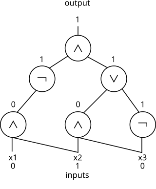
In computational complexity theory and circuit complexity, a Boolean circuit is a mathematical model for combinational digital logic circuits. A formal language can be decided by a family of Boolean circuits, one circuit for each possible input length.

<span class="mw-page-title-main">Circuit complexity</span> Model of computational complexity

In theoretical computer science, circuit complexity is a branch of computational complexity theory in which Boolean functions are classified according to the size or depth of the Boolean circuits that compute them. A related notion is the circuit complexity of a recursive language that is decided by a uniform family of circuits .

<span class="mw-page-title-main">Karnaugh map</span> Graphical method to simplify Boolean expressions

The Karnaugh(/ˈkɑːnɔː/) map is a method of simplifying Boolean algebra expressions. Maurice Karnaugh introduced it in 1953 as a refinement of Edward W. Veitch's 1952 Veitch chart, which itself was a rediscovery of Allan Marquand's 1881 logical diagram aka Marquand diagram but now with a focus set on its utility for switching circuits. Veitch charts are also known as Marquand–Veitch diagrams, Svoboda charts -(albeit only rarely)- and even Karnaugh maps as Karnaugh–Veitch maps.

Zhegalkinpolynomials, also known as algebraic normal form, are a representation of functions in Boolean algebra. Introduced by the Russian mathematician Ivan Ivanovich Zhegalkin in 1927, they are the polynomial ring over the integers modulo 2. The resulting degeneracies of modular arithmetic result in Zhegalkin polynomials being simpler than ordinary polynomials, requiring neither coefficients nor exponents. Coefficients are redundant because 1 is the only nonzero coefficient. Exponents are redundant because in arithmetic mod 2, x2 = x. Hence a polynomial such as 3x2y5z is congruent to, and can therefore be rewritten as, xyz.

In theoretical computer science, a circuit is a model of computation in which input values proceed through a sequence of gates, each of which computes a function. Circuits of this kind provide a generalization of Boolean circuits and a mathematical model for digital logic circuits. Circuits are defined by the gates they contain and the values the gates can produce. For example, the values in a Boolean circuit are boolean values, and the circuit includes conjunction, disjunction, and negation gates. The values in an integer circuit are sets of integers and the gates compute set union, set intersection, and set complement, as well as the arithmetic operations addition and multiplication.

In theoretical computer science, the circuit satisfiability problem is the decision problem of determining whether a given Boolean circuit has an assignment of its inputs that makes the output true. In other words, it asks whether the inputs to a given Boolean circuit can be consistently set to 1 or 0 such that the circuit outputs 1. If that is the case, the circuit is called satisfiable. Otherwise, the circuit is called unsatisfiable. In the figure to the right, the left circuit can be satisfied by setting both inputs to be 1, but the right circuit is unsatisfiable.

In mathematics and mathematical logic, Boolean algebra is a branch of algebra. It differs from elementary algebra in two ways. First, the values of the variables are the truth values true and false, usually denoted 1 and 0, whereas in elementary algebra the values of the variables are numbers. Second, Boolean algebra uses logical operators such as conjunction (and) denoted as , disjunction (or) denoted as , and the negation (not) denoted as ¬. Elementary algebra, on the other hand, uses arithmetic operators such as addition, multiplication, subtraction, and division. Boolean algebra is therefore a formal way of describing logical operations, in the same way that elementary algebra describes numerical operations.

References

  1. Peter J. Pahl; Rudolf Damrath (2012-12-06). Mathematical Foundations of Computational Engineering: A Handbook. Springer Science & Business Media. pp. 15–. ISBN   978-3-642-56893-0.
  2. Lala, Parag K. (2007-07-16). Principles of Modern Digital Design. John Wiley & Sons. p. 78. ISBN   978-0-470-07296-7.
  3. Hall, Eldon C. (1996). Journey to the Moon: The History of the Apollo Guidance Computer. AIAA. ISBN   1-56347-185-X.
  4. "APOLLO GUIDANCE COMPUTER (AGC) Schematics". klabs.org. Rich Katz. Retrieved 2021-06-19. To see how NOR gate logic was used in the Apollo Guidance Computer's ALU, select any of the 4-BIT MODULE entries in the Index to Drawings, and expand images as desired.

Further reading