
In microelectronics, a dual in-line package is an electronic component package with a rectangular housing and two parallel rows of electrical connecting pins. The package may be through-hole mounted to a printed circuit board (PCB) or inserted in a socket. The dual-inline format was invented by Don Forbes, Rex Rice and Bryant Rogers at Fairchild R&D in 1964, when the restricted number of leads available on circular transistor-style packages became a limitation in the use of integrated circuits. Increasingly complex circuits required more signal and power supply leads ; eventually microprocessors and similar complex devices required more leads than could be put on a DIP package, leading to development of higher-density chip carriers. Furthermore, square and rectangular packages made it easier to route printed-circuit traces beneath the packages.

A printed circuit board (PCB), also called printed wiring board (PWB), is a medium used to connect or "wire" components to one another in a circuit. It takes the form of a laminated sandwich structure of conductive and insulating layers: each of the conductive layers is designed with an artwork pattern of traces, planes and other features etched from one or more sheet layers of copper laminated onto and/or between sheet layers of a non-conductive substrate. Electrical components may be fixed to conductive pads on the outer layers in the shape designed to accept the component's terminals, generally by means of soldering, to both electrically connect and mechanically fasten them to it. Another manufacturing process adds vias: plated-through holes that allow interconnections between layers.

A ball grid array (BGA) is a type of surface-mount packaging used for integrated circuits. BGA packages are used to permanently mount devices such as microprocessors. A BGA can provide more interconnection pins than can be put on a dual in-line or flat package. The whole bottom surface of the device can be used, instead of just the perimeter. The traces connecting the package's leads to the wires or balls which connect the die to package are also on average shorter than with a perimeter-only type, leading to better performance at high speeds.

Flip chip, also known as controlled collapse chip connection or its abbreviation, C4, is a method for interconnecting dies such as semiconductor devices, IC chips, integrated passive devices and microelectromechanical systems (MEMS), to external circuitry with solder bumps that have been deposited onto the chip pads. The technique was developed by General Electric's Light Military Electronics Department, Utica, New York. The solder bumps are deposited on the chip pads on the top side of the wafer during the final wafer processing step. In order to mount the chip to external circuitry, it is flipped over so that its top side faces down, and aligned so that its pads align with matching pads on the external circuit, and then the solder is reflowed to complete the interconnect. This is in contrast to wire bonding, in which the chip is mounted upright and fine wires are welded onto the chip pads and lead frame contacts to interconnect the chip pads to external circuitry.

Depaneling is a process step in high-volume electronics assembly production. In order to increase the throughput of printed circuit board (PCB) manufacturing and surface mount (SMT) lines, PCBs are often designed so that they consist of many smaller individual PCBs that will be used in the final product. This PCB cluster is called a panel or multiblock. The large panel is broken up or "depaneled" as a certain step in the process - depending on the product, it may happen right after SMT process, after in-circuit test (ICT), after soldering of through-hole elements, or even right before the final assembly of the PCBA into the enclosure.

Automatic test equipment or automated test equipment (ATE) is any apparatus that performs tests on a device, known as the device under test (DUT), equipment under test (EUT) or unit under test (UUT), using automation to quickly perform measurements and evaluate the test results. An ATE can be a simple computer-controlled digital multimeter, or a complicated system containing dozens of complex test instruments capable of automatically testing and diagnosing faults in sophisticated electronic packaged parts or on wafer testing, including system on chips and integrated circuits.

In-system programming (ISP), or also called in-circuit serial programming (ICSP), is the ability of some programmable logic devices, microcontrollers, chipsets and other embedded devices to be programmed while installed in a complete system, rather than requiring the chip to be programmed prior to installing it into the system. It also allows firmware updates to be delivered to the on-chip memory of microcontrollers and related processors without requiring specialist programming circuitry on the circuit board, and simplifies design work.
A device under test (DUT), also known as equipment under test (EUT) and unit under test (UUT), is a manufactured product undergoing testing, either at first manufacture or later during its life cycle as part of ongoing functional testing and calibration checks. This can include a test after repair to establish that the product is performing in accordance with the original product specification.
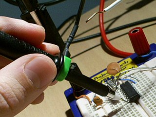
A test probe is a physical device used to connect electronic test equipment to a device under test (DUT). Test probes range from very simple, robust devices to complex probes that are sophisticated, expensive, and fragile. Specific types include test prods, oscilloscope probes and current probes. A test probe is often supplied as a test lead, which includes the probe, cable and terminating connector.

A probe card is used in automated integrated circuit testing. It is an interface between an electronic test system and a semiconductor wafer.
A Fuzz Button is a high performance electrical connection material used to connect two parts of an electrical circuit together, for example an IC to a PCB or two PCBs to each other. Fuzz Buttons consist of a single strand of gold-plated beryllium copper wire compressed into a dense, sponge-like cylindrical shape. Their diameter can range from a few tenths of a millimetre to a millimetre.
SPEA is an Italian company that designs and manufactures Automatic Test Equipment (ATE) for testing MEMS, Sensors, microchips and Printed circuit board.
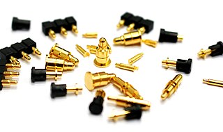
A pogo pin or spring-loaded pin is a type of electrical connector mechanism that is used in many modern electronic applications and in the electronics testing industry. They are used for their improved durability over other electrical contacts, and the resilience of their electrical connection to mechanical shock and vibration.
In-circuit testing (ICT) is an example of white box testing where an electrical probe tests a populated printed circuit board (PCB), checking for shorts, opens, resistance, capacitance, and other basic quantities which will show whether the assembly was correctly fabricated. It may be performed with a "bed of nails" test fixture and specialist test equipment, or with a fixtureless in-circuit test setup.
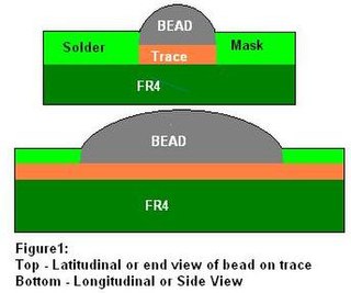
Bead probe technology (BPT) is technique used to provide electrical access to printed circuit board (PCB) circuitry for performing in-circuit testing (ICT). It makes use of small beads of solder placed onto the board's traces to allow measuring and controlling of the signals using a test probe. This permits test access to boards on which standard ICT test pads are not feasible due to space constraints.
In the manufacture of electronic printed circuit boards, flying probes are used for testing both bare circuit boards and boards loaded with components. Flying probes were introduced in the late 1980’s. Flying probes can be found in many manufacturing and assembly operations. A flying probe tester uses one or more test probes to make contact with the circuit board under test; the probes are moved from place to place on the circuit board to carry out tests of multiple conductors or components. Flying probe testers are an alternative to bed of nails testers, which use multiple contacts to simultaneously contact the board and which rely on electrical switching to carry out measurements.
A semiconductor package is a metal, plastic, glass, or ceramic casing containing one or more discrete semiconductor devices or integrated circuits. Individual components are fabricated on semiconductor wafers before being diced into die, tested, and packaged. The package provides a means for connecting it to the external environment, such as printed circuit board, via leads such as lands, balls, or pins; and protection against threats such as mechanical impact, chemical contamination, and light exposure. Additionally, it helps dissipate heat produced by the device, with or without the aid of a heat spreader. There are thousands of package types in use. Some are defined by international, national, or industry standards, while others are particular to an individual manufacturer.
Circuit Check is an American company with about 225 employees and seven direct operations in six countries. Headquartered in Maple Grove, Minnesota, it is one of the largest manufacturers of electronic and mechanical test fixtures in North America, . The company also manufactures Automatic Test Equipment for end-of-line manufacturing test. The company uses either a Microsoft Excel-driven "CCITest" software platform, or the National Instruments LabVIEW software platform. They have a variety of clients in different industries which include: Automotive, Military & Aerospace, Medical, Industrial, and Computer Networking.
Pad cratering is a mechanically induced fracture in the resin between copper foil and outermost layer of fiberglass of a printed circuit board (PCB). It may be within the resin or at the resin to fiberglass interface.
Dye-n-Pry, also called Dye And Pry, Dye and Pull, Dye Staining, or Dye Penetrant, is a destructive analysis technique used on surface mount technology (SMT) components to either perform failure analysis or inspect for solder joint integrity. It is an application of dye penetrant inspection.
