Boundary scan

Last updated
JTAG Register.svg

Boundary scan is a method for testing interconnects (wire lines) on printed circuit boards or sub-blocks inside an integrated circuit. Boundary scan is also widely used as a debugging method to watch integrated circuit pin states, measure voltage, or analyze sub-blocks inside an integrated circuit.

Contents

The Joint Test Action Group (JTAG) developed a specification for boundary scan testing that was standardized in 1990 as the IEEE Std. 1149.1-1990. In 1994, a supplement that contains a description of the Boundary Scan Description Language (BSDL) was added which describes the boundary-scan logic content of IEEE Std 1149.1 compliant devices. Since then, this standard has been adopted by electronic device companies all over the world. Boundary scan is now mostly synonymous with JTAG. [1] [2]

Testing

The boundary scan architecture provides a means to test interconnects (including clusters of logic, memories, etc.) without using physical test probes; this involves the addition of at least one test cell that is connected to each pin of the device and that can selectively override the functionality of that pin. Each test cell may be programmed via the JTAG scan chain to drive a signal onto a pin and thus across an individual trace on the board; the cell at the destination of the board trace can then be read, verifying that the board trace properly connects the two pins. If the trace is shorted to another signal or if the trace is open, the correct signal value does not show up at the destination pin, indicating a fault.

On-chip infrastructure

To provide the boundary scan capability, IC vendors add additional logic to each of their devices, including scan cells for each of the external traces. These cells are then connected together to form the external boundary scan shift register (BSR), and combined with JTAG Test Access Port (TAP) controller support comprising four (or sometimes more) additional pins plus control circuitry.

Some TAP controllers support scan chains between on-chip logical design blocks, with JTAG instructions which operate on those internal scan chains instead of the BSR. This can allow those integrated components to be tested as if they were separate chips on a board. On-chip debugging solutions are heavy users of such internal scan chains.

These designs are part of most Verilog or VHDL libraries. Overhead for this additional logic is minimal, and generally is well worth the price to enable efficient testing at the board level.

For normal operation, the added boundary scan latch cells are set so that they have no effect on the circuit, and are therefore effectively invisible. However, when the circuit is set into a test mode, the latches enable a data stream to be shifted from one latch into the next. Once a complete data word has been shifted into the circuit under test, it can be latched into place so it drives external signals. Shifting the word also generally returns the input values from the signals configured as inputs.

Test mechanism

As the cells can be used to force data into the board, they can set up test conditions. The relevant states can then be fed back into the test system by clocking the data word back so that it can be analyzed.

By adopting this technique, it is possible for a test system to gain test access to a board. As most of today's boards are very densely populated with components and tracks, it is very difficult for test systems to physically access the relevant areas of the board to enable them to test the board. Boundary scan makes access possible without always needing physical probes.

In modern chip and board design, Design For Test is a significant issue, and one common design artifact is a set of boundary scan test vectors, possibly delivered in Serial Vector Format (SVF) or a similar interchange format.

JTAG test operations

Devices communicate to the world via a set of input and output pins. By themselves, these pins provide limited visibility into the workings of the device. However, devices that support boundary scan contain a shift-register cell for each signal pin of the device. These registers are connected in a dedicated path around the device's boundary (hence the name). The path creates a virtual access capability that circumvents the normal inputs and provides direct control of the device and detailed visibility at its outputs. [3] The contents of the boundary scan are usually described by the manufacturer using a part-specific BSDL file.

Among other things, a BSDL file will describe each digital signal exposed through pin or ball (depending on the chip packaging) exposed in the boundary scan, as part of its definition of the Boundary Scan Register (BSR). A description for two balls might look like this:

"541 (bc_1,                     *,  control,  1),"&"542 (bc_1,         GPIO51_ATACS1,  output3,  X,    541,   1,   Z),"&"543 (bc_1,         GPIO51_ATACS1,    input,  X),"&"544 (bc_1,                     *,  control,  1),"&"545 (bc_1,         GPIO50_ATACS0,  output3,  X,    544,   1,   Z),"&"546 (bc_1,         GPIO50_ATACS0,    input,  X),"&

That shows two balls on a mid-size chip (the boundary scan includes about 620 such lines, in a 361-ball BGA package), each of which has three components in the BSR: a control configuring the ball (as input, output, what drive level, pullups, pulldowns, and so on); one type of output signal; and one type of input signal.

There are JTAG instructions to SAMPLE the data in that boundary scan register, or PRELOAD it with values.

During testing, I/O signals enter and leave the chip through the boundary-scan cells. Testing involves a number of test vectors, each of which drives some signals and then verifies that the responses are as expected. The boundary-scan cells can be configured to support external testing for interconnection between chips (EXTEST instruction) or internal testing for logic within the chip (INTEST instruction).

Board test infrastructure

Typically high-end commercial JTAG testing systems allow the import of design 'netlists' from CAD/EDA systems plus the BSDL models of boundary scan/JTAG compliant devices to automatically generate test applications. Common types of test include

When used during manufacturing, such systems also support non-test but affiliated applications such as in-system programming of various types of flash memory: NOR, NAND, and serial (I2C or SPI).

Such commercial systems are used by board test professionals and will often cost several thousand dollars for a fully-fledged system. They can include diagnostic options to accurately pin-point faults such as open circuits and shorts and may also offer schematic or layout viewers to depict the fault in a graphical manner. Tests developed with such tools are frequently combined with other test systems such as in-circuit testers (ICTs) or functional board test systems.

Debugging

The boundary scan architecture also provides functionality which helps developers and engineers during development stages of an embedded system. A JTAG Test Access Port (TAP) can be turned into a low-speed logic analyzer.

History

James B. Angell at Stanford University proposed serial testing. [4]

IBM developed level-sensitive scan design (LSSD). [5] [6]

See also

Related Research Articles

<span class="mw-page-title-main">Digital electronics</span> Electronic circuits that utilize digital signals

Digital electronics is a field of electronics involving the study of digital signals and the engineering of devices that use or produce them. This is in contrast to analog electronics and analog signals.

<span class="mw-page-title-main">Programmable logic device</span> Reconfigurable digital circuit element

A programmable logic device (PLD) is an electronic component used to build reconfigurable digital circuits. Unlike digital logic constructed using discrete logic gates with fixed functions, a PLD has an undefined function at the time of manufacture. Before the PLD can be used in a circuit it must be programmed to implement the desired function. Compared to fixed logic devices, programmable logic devices simplify the design of complex logic and may offer superior performance. Unlike for microprocessors, programming a PLD changes the connections made between the gates in the device.

<span class="mw-page-title-main">AVR microcontrollers</span> Family of microcontrollers

AVR is a family of microcontrollers developed since 1996 by Atmel, acquired by Microchip Technology in 2016. These are modified Harvard architecture 8-bit RISC single-chip microcontrollers. AVR was one of the first microcontroller families to use on-chip flash memory for program storage, as opposed to one-time programmable ROM, EPROM, or EEPROM used by other microcontrollers at the time.

In electronics and especially synchronous digital circuits, a clock signal is an electronic logic signal which oscillates between a high and a low state at a constant frequency and is used like a metronome to synchronize actions of digital circuits. In a synchronous logic circuit, the most common type of digital circuit, the clock signal is applied to all storage devices, flip-flops and latches, and causes them all to change state simultaneously, preventing race conditions.

<span class="mw-page-title-main">Ball grid array</span> Surface-mount packaging that uses an array of solder balls

A ball grid array (BGA) is a type of surface-mount packaging used for integrated circuits. BGA packages are used to permanently mount devices such as microprocessors. A BGA can provide more interconnection pins than can be put on a dual in-line or flat package. The whole bottom surface of the device can be used, instead of just the perimeter. The traces connecting the package's leads to the wires or balls which connect the die to package are also on average shorter than with a perimeter-only type, leading to better performance at high speeds.

Serial Peripheral Interface (SPI) is a de facto standard for synchronous serial communication, used primarily in embedded systems for short-distance wired communication between integrated circuits.

JTAG is an industry standard for verifying designs and testing printed circuit boards after manufacture.

Design for testing or design for testability (DFT) consists of IC design techniques that add testability features to a hardware product design. The added features make it easier to develop and apply manufacturing tests to the designed hardware. The purpose of manufacturing tests is to validate that the product hardware contains no manufacturing defects that could adversely affect the product's correct functioning.

In computer architecture, clock gating is a popular power management technique used in many synchronous circuits for reducing dynamic power dissipation, by removing the clock signal when the circuit is not in use or ignores clock signal. Clock gating saves power by pruning the clock tree, at the cost of adding more logic to a circuit. Pruning the clock disables portions of the circuitry so that the flip-flops in them do not have to switch states. Switching states consumes power. When not being switched, the switching power consumption goes to zero, and only leakage currents are incurred.

<span class="mw-page-title-main">In-system programming</span> Embedded system programming technique

In-system programming (ISP), or also called in-circuit serial programming (ICSP), is the ability of some programmable logic devices, microcontrollers, chipsets and other embedded devices to be programmed while installed in a complete system, rather than requiring the chip to be programmed prior to installing it into the system. It also allows firmware updates to be delivered to the on-chip memory of microcontrollers and related processors without requiring specialist programming circuitry on the circuit board, and simplifies design work.

<span class="mw-page-title-main">Integrated circuit design</span> Engineering process for electronic hardware

Integrated circuit design, or IC design, is a sub-field of electronics engineering, encompassing the particular logic and circuit design techniques required to design integrated circuits, or ICs. ICs consist of miniaturized electronic components built into an electrical network on a monolithic semiconductor substrate by photolithography.

Boundary scan description language (BSDL) is a hardware description language for electronics testing using JTAG. It has been added to the IEEE Std. 1149.1, and BSDL files are increasingly well supported by JTAG tools for boundary scan applications, and by test case generators.

Serial Vector Format (SVF) is a file format that contains boundary scan vectors to be sent to an electronic circuit using a JTAG interface. Boundary scan vectors consist of the following data:

In-circuit testing (ICT) is an example of white box testing where an electrical probe tests a populated printed circuit board (PCB), checking for shorts, opens, resistance, capacitance, and other basic quantities which will show whether the assembly was correctly fabricated. It may be performed with a "bed of nails" test fixture and specialist test equipment, or with a fixtureless in-circuit test setup.

<span class="mw-page-title-main">Intel 8255</span>

The Intel 8255 Programmable Peripheral Interface (PPI) chip was developed and manufactured by Intel in the first half of the 1970s for the Intel 8080 microprocessor. The 8255 provides 24 parallel input/output lines with a variety of programmable operating modes.

<span class="mw-page-title-main">Bead probe technology</span> Technique used for in-circuit testing

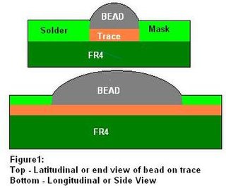
Bead probe technology (BPT) is technique used to provide electrical access to printed circuit board (PCB) circuitry for performing in-circuit testing (ICT). It makes use of small beads of solder placed onto the board's traces to allow measuring and controlling of the signals using a test probe. This permits test access to boards on which standard ICT test pads are not feasible due to space constraints.

<span class="mw-page-title-main">Hardware Trojan</span> Malware embedded in hardware; harder to detect and fix than software vulnerabilities

A Hardware Trojan (HT) is a malicious modification of the circuitry of an integrated circuit. A hardware Trojan is completely characterized by its physical representation and its behavior. The payload of an HT is the entire activity that the Trojan executes when it is triggered. In general, Trojans try to bypass or disable the security fence of a system: for example, leaking confidential information by radio emission. HTs also could disable, damage or destroy the entire chip or components of it.

<span class="mw-page-title-main">Flip-flop (electronics)</span> Electronic circuit with two stable states

In electronics, flip-flops and latches are circuits that have two stable states that can store state information – a bistable multivibrator. The circuit can be made to change state by signals applied to one or more control inputs and will output its state. It is the basic storage element in sequential logic. Flip-flops and latches are fundamental building blocks of digital electronics systems used in computers, communications, and many other types of systems.

In the electronics industry, embedded instrumentation refers to the integration of test and measurement instrumentation into semiconductor chips. Embedded instrumentation differs from embedded system, which are electronic systems or subsystems that usually comprise the control portion of a larger electronic system. Instrumentation embedded into chips is employed in a variety of electronic test applications, including validating and testing chips themselves, validating, testing and debugging the circuit boards where these chips are deployed, and troubleshooting systems once they have been installed in the field.

MIPI Alliance Debug Architecture provides a standardized infrastructure for debugging deeply embedded systems in the mobile and mobile-influenced space. The MIPI Alliance MIPI Debug Working Group has released a portfolio of specifications; their objective is to provide standard debug protocols and standard interfaces from a system on a chip (SoC) to the debug tool. The whitepaper Architecture Overview for Debug summarizes all the efforts. In recent years, the group focused on specifying protocols that improve the visibility of the internal operations of deeply embedded systems, standardizing debug solutions via the functional interfaces of form factor devices, and specifying the use of I3C as debugging bus.

References

  1. IEEE Std 1149.1 (JTAG) Testability Primer Chapter 3 covers boundary scan with JTAG, and other chapters are also informative.
  2. Frenzel, Louis E. (September 11, 2008). "The Embedded Plan For JTAG Boundary Scan". Electronic Design . Archived from the original on 2008-12-01. presents an overview, circa 2008.
  3. Oshana, Rob (October 29, 2002). "Introduction to JTAG". Embedded Systems Design. Retrieved 2007-04-05.
  4. Williams, M. J. Y.; Angel, J. B. (January 1973), "Enhancing Testability of Large Scale Integrated Circuits via Test Points and Additional Logic", IEEE Transactions on Computers, C-22 (1): 46–60, doi:10.1109/T-C.1973.223600, S2CID   5427856
  5. US 3761695,Eichelberger, Edward,"Method of Level Sensitive Testing a Functional Logic System",issued 9/25/1973
  6. US 4293919,Dasgupta, Sumit,"Level sensitive scan design (LSSD) system",issued 10/06/1981