Index register

Last updated
Index register display on an IBM 7094 mainframe from the early 1960s IBM 7094 console.agr.JPG
Index register display on an IBM 7094 mainframe from the early 1960s

An index register in a computer's CPU is a processor register (or an assigned memory location) [1] used for pointing to operand addresses during the run of a program. It is useful for stepping through strings and arrays. It can also be used for holding loop iterations and counters. In some architectures it is used for read/writing blocks of memory. Depending on the architecture it may be a dedicated index register or a general-purpose register. [2] Some instruction sets allow more than one index register to be used; in that case additional instruction fields may specify which index registers to use. [3]

Contents

Generally, the contents of an index register is added to (in some cases subtracted from) an immediate address (that can be part of the instruction itself or held in another register) to form the "effective" address of the actual data (operand). Special instructions are typically provided to test the index register and, if the test fails, increments the index register by an immediate constant and branches, typically to the start of the loop. While normally processors that allow an instruction to specify multiple index registers add the contents together, IBM had a line of computers in which the contents were or'd together. [4]

Index registers has proved useful for doing vector/array operations and in commercial data processing for navigating from field to field within records. In both uses index registers substantially reduced the amount of memory used and increased execution speed.

History

In early computers without any form of indirect addressing, array operations had to be performed by modifying the instruction address, which required several additional program steps and used up more computer memory, [5] a scarce resource in computer installations of the early era (as well as in early microcomputers two decades later).

Index registers, commonly known as B-lines in early British computers, as B-registers on some machines and a X-registers [lower-alpha 1] on others, were first used in the British Manchester Mark 1 computer, in 1949. In general, index registers became a standard part of computers during the technology's second generation, roughly 19541966. Most [lower-alpha 2] machines in the IBM 700/7000 mainframe series had them, starting with the IBM 704 in 1954, though they were optional on some smaller machines such as the IBM 650 and IBM 1401.

Early "small machines" with index registers include the AN/USQ-17, around 1960, and the 9 series of real-time computers from Scientific Data Systems, from the early 1960s.

The 1962 UNIVAC 1107 has 15 X-registers, four of which were also A-registers.

The 1964 GE-635 has 8 dedicated X-registers; however, it also allows indexing by the instruction counter or by either half of the A or Q register.

The Digital Equipment Corporation (DEC) PDP-6, introduced in 1964, and the IBM System/360, announced in 1964, do not include dedicated index registers; instead, they have general-purpose registers (called "accumulators" in the PDP-6) that can contain either numerical values or addresses. The memory address of an operand is, in the PDP-6, the sum of the contents of a general-purpose register and an 18-bit offset and, on the System/360, the sum of the contents of two general-purpose registers and a 12-bit offset. [6] [7] The compatible PDP-10 line of successors to the PDP-6, and the IBM System/370 and later compatible successors to the System/360, including the current z/Architecture, work in the same fashion.

The 1969 Data General Nova and successor Eclipse, and 1970 DEC PDP-11, minicomputers also provided general-purpose registers (called "accumulators" in the Nova and Eclipse), rather than separate accumulators and index registers, as did their Eclipse MV and VAX 32-bit superminicomputer successors. In the PDP-11 and VAX, any register could be used when calculating the memory address of an operand; in the Nova, Eclipse, and Eclipse MV, only registers 2 and 3 could be used. [8] [9] [10]

The 1971 CDC STAR-100 has a register file of 256 64-bit registers, 9 of which are reserved. Unlike most computers, the STAR-100 instructions only have register fields and operand fields, so the registers serve more as pointer registers than as traditional index registers.

While the 1972 Intel 8008 allowed indirect addressing via register pairs, the first microprocessor with a true index register appears to have been the 1974 Motorola 6800.

In 1975, the 8-bit MOS Technology 6502 processor had two index registers 'X' and 'Y'. [11]

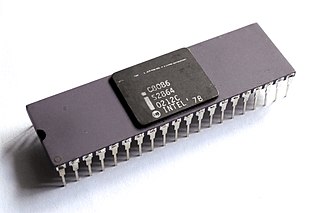
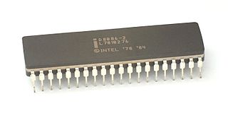
In 1978, the Intel 8086, the first x86 processor, had eight 16-bit registers, referred to as "general-purpose", all of which can be used as integer data registers in most operations; four of them, 'SI' (source index), 'DI' (destination index), 'BX' (base), and 'BP' (base pointer), can also be used when computing the memory address of an operand, which is the sum of one of those registers and a displacement, or the sum of one of 'BX' or 'BP", one of 'SI' or 'DI', and a displacement. [12] The 1979 Intel 8088, and the 16-bit Intel 80186, Intel 80188, and Intel 80286 successors work the same. In 1985, the i386, a 32-bit successor to those processors, introducing the IA-32 32-bit version of the x86 architecture, extended the eight 16-bit registers to 32 bits, with "E" added to the beginning of the register name; in IA-32, the memory address of an operand is the sum of one of those eight registers, one of seven of those registers (the stack pointer is not allowed as the second register here) multiplied by 1, 2, 4, or 8, and a displacement. [13] :3-11–3-12,3-22–3-23 The Advanced Micro Devices Opteron, the first model of which was released in 2003, introduced x86-64, the 64-bit version of the x86 instruction set; in x86-64, the general-purpose registers were extended to 64 bits, and eight additional general-purpose registers were added; the memory address of an operand is the sum of two of those 16 registers and a displacement. [14] [13] :3–12,3–24

The reduced instruction set computing (RISC) instruction sets introduced in the 1980s and 1990s all provide general-purpose registers that can contain either numerical values or address values. In most of those instruction sets, there are 32 general-purpose registers (in some of those instruction sets, the value of one of those registers is hardwired to zero) could be used to calculate the operand address; they did not have dedicated index registers. In the 32-bit version of the ARM architecture, first developed in 1985, there are 16 registers designated as "general-purpose registers", but only 13 of them can be used for all purposes, with register R15 containing the program counter. The memory address of a load or store instruction is the sum of any of the 16 registers and either a displacement or another of the registers with the exception of R15 (possibly shifted left for scaling). [15] In the 64-bit version of the ARM architecture, there are 31 64-bit general-purpose registers plus a stack pointer and a zero register; the memory address of a load or store instruction is the sum of any of the 31 registers and either a displacement or another of the registers. [16]

Examples

Here is a simple example of index register use in assembly language pseudo-code that sums a 100 entry array of 4-byte words:

   Clear_accumulator    Load_index 400,index2  //load 4*array size into index register 2 (index2) loop_start : Add_word_to_accumulator array_start,index2   //Add to AC the word at the address (array_start + index2)    Branch_and_decrement_if_index_not_zero loop_start,4,index2   //loop decrementing by 4 until index register is zero

See also

Notes

  1. The term X-registers was also used for accumulators on, e.g., the CDC 6600.
  2. The 702, 705 and 7080 did not have index registers.

Related Research Articles

<span class="mw-page-title-main">Accumulator (computing)</span> Register in which intermediate arithmetic and logic results of a CPU are stored

In a computer's central processing unit (CPU), the accumulator is a register in which intermediate arithmetic logic unit results are stored.

IA-32 is the 32-bit version of the x86 instruction set architecture, designed by Intel and first implemented in the 80386 microprocessor in 1985. IA-32 is the first incarnation of x86 that supports 32-bit computing; as a result, the "IA-32" term may be used as a metonym to refer to all x86 versions that support 32-bit computing.

<span class="mw-page-title-main">Intel 8086</span> 16-bit microprocessor

The 8086 is a 16-bit microprocessor chip designed by Intel between early 1976 and June 8, 1978, when it was released. The Intel 8088, released July 1, 1979, is a slightly modified chip with an external 8-bit data bus, and is notable as the processor used in the original IBM PC design.

<span class="mw-page-title-main">Machine code</span> Set of instructions executed by a computer

In computer programming, machine code is computer code consisting of machine language instructions, which are used to control a computer's central processing unit (CPU). Although decimal computers were once common, the contemporary marketplace is dominated by binary computers; for those computers, machine code is "the binary representation of a computer program which is actually read and interpreted by the computer. A program in machine code consists of a sequence of machine instructions ."

x86 Family of instruction set architectures

x86 is a family of complex instruction set computer (CISC) instruction set architectures initially developed by Intel based on the Intel 8086 microprocessor and its 8088 variant. The 8086 was introduced in 1978 as a fully 16-bit extension of Intel's 8-bit 8080 microprocessor, with memory segmentation as a solution for addressing more memory than can be covered by a plain 16-bit address. The term "x86" came into being because the names of several successors to Intel's 8086 processor end in "86", including the 80186, 80286, 80386 and 80486 processors. Colloquially, their names were "186", "286", "386" and "486".

<span class="mw-page-title-main">Endianness</span> Order of bytes in a computer word

In computing, endianness is the order in which bytes within a word of digital data are transmitted over a data communication medium or addressed in computer memory, counting only byte significance compared to earliness. Endianness is primarily expressed as big-endian (BE) or little-endian (LE), terms introduced by Danny Cohen into computer science for data ordering in an Internet Experiment Note published in 1980. The adjective endian has its origin in the writings of 18th century Anglo-Irish writer Jonathan Swift. In the 1726 novel Gulliver's Travels, he portrays the conflict between sects of Lilliputians divided into those breaking the shell of a boiled egg from the big end or from the little end. By analogy, a CPU may read a digital word big end first, or little end first.

In computer science, an instruction set architecture (ISA) is a part of the abstract model of a computer, which generally defines how software controls the CPU. A device that executes instructions described by that ISA, such as a central processing unit (CPU), is called an implementation.

<span class="mw-page-title-main">MCS-51</span> Single chip microcontroller series by Intel

The Intel MCS-51 is a single chip microcontroller (MCU) series developed by Intel in 1980 for use in embedded systems. The architect of the Intel MCS-51 instruction set was John H. Wharton. Intel's original versions were popular in the 1980s and early 1990s, and enhanced binary compatible derivatives remain popular today. It is a complex instruction set computer, but also has some of the features of RISC architectures, such as a large register set and register windows, and has separate memory spaces for program instructions and data.

In computer architecture, 64-bit integers, memory addresses, or other data units are those that are 64 bits wide. Also, 64-bit central processing units (CPU) and arithmetic logic units (ALU) are those that are based on processor registers, address buses, or data buses of that size. A computer that uses such a processor is a 64-bit computer.

x86 assembly language is the name for the family of assembly languages which provide some level of backward compatibility with CPUs back to the Intel 8008 microprocessor, which was launched in April 1972. It is used to produce object code for the x86 class of processors.

Memory-mapped I/O (MMIO) and port-mapped I/O (PMIO) are two complementary methods of performing input/output (I/O) between the central processing unit (CPU) and peripheral devices in a computer. An alternative approach is using dedicated I/O processors, commonly known as channels on mainframe computers, which execute their own instructions.

A processor register is a quickly accessible location available to a computer's processor. Registers usually consist of a small amount of fast storage, although some registers have specific hardware functions, and may be read-only or write-only. In computer architecture, registers are typically addressed by mechanisms other than main memory, but may in some cases be assigned a memory address e.g. DEC PDP-10, ICT 1900.

Addressing modes are an aspect of the instruction set architecture in most central processing unit (CPU) designs. The various addressing modes that are defined in a given instruction set architecture define how the machine language instructions in that architecture identify the operand(s) of each instruction. An addressing mode specifies how to calculate the effective memory address of an operand by using information held in registers and/or constants contained within a machine instruction or elsewhere.

Byte addressing in hardware architectures supports accessing individual bytes. Computers with byte addressing are sometimes called byte machines, in contrast to word-addressable architectures, word machines, that access data by word.

In computer engineering, an orthogonal instruction set is an instruction set architecture where all instruction types can use all addressing modes. It is "orthogonal" in the sense that the instruction type and the addressing mode vary independently. An orthogonal instruction set does not impose a limitation that requires a certain instruction to use a specific register so there is little overlapping of instruction functionality.

In computing, a word is the natural unit of data used by a particular processor design. A word is a fixed-sized datum handled as a unit by the instruction set or the hardware of the processor. The number of bits or digits in a word is an important characteristic of any specific processor design or computer architecture.

A stack register is a computer central processor register whose purpose is to keep track of a call stack. On an accumulator-based architecture machine, this may be a dedicated register. On a machine with multiple general-purpose registers, it may be a register that is reserved by convention, such as on the IBM System/360 through z/Architecture architecture and RISC architectures, or it may be a register that procedure call and return instructions are hardwired to use, such as on the PDP-11, VAX, and Intel x86 architectures. Some designs such as the Data General Eclipse had no dedicated register, but used a reserved hardware memory address for this function.

An instruction set architecture (ISA) is an abstract model of a computer, also referred to as computer architecture. A realization of an ISA is called an implementation. An ISA permits multiple implementations that may vary in performance, physical size, and monetary cost ; because the ISA serves as the interface between software and hardware. Software that has been written for an ISA can run on different implementations of the same ISA. This has enabled binary compatibility between different generations of computers to be easily achieved, and the development of computer families. Both of these developments have helped to lower the cost of computers and to increase their applicability. For these reasons, the ISA is one of the most important abstractions in computing today.

In computer engineering, a register–memory architecture is an instruction set architecture that allows operations to be performed on memory, as well as registers. If the architecture allows all operands to be in memory or in registers, or in combinations, it is called a "register plus memory" architecture.

The EVEX prefix and corresponding coding scheme is an extension to the 32-bit x86 (IA-32) and 64-bit x86-64 (AMD64) instruction set architecture. EVEX is based on, but should not be confused with the MVEX prefix used by the Knights Corner processor.

References

  1. "Instructions: Index Words" (PDF). IBM 7070-7074 Principles of Operation (PDF). IBM. 1962. p. 11. GA22-7003-6.
  2. "What Is an Index Register? (with picture)". EasyTechJunkie. Retrieved 2022-07-24.
  3. IBM 709 Reference Manual, Form A22-6501-0, 1958, p. 12
  4. IBM 7094 Principles of Operation (PDF). Fifth Edition. IBM. October 21, 1966. A22-6703-4.
  5. IBM 1401 Reference manual, Form A24-1403-4, 1960, p. 77
  6. Programmed Data Processor-6 Handbook (PDF). Digital Equipment Corporation. August 1964. pp. 20–22.
  7. IBM System/360 Principles of Operation (PDF) (Eighth ed.). IBM. September 1968. pp. 8, 12–14. A22-6821-7.
  8. Programmer's Reference Manual, Nova Line Computers (PDF). Data General. January 1976. pp. I-1, II-7.
  9. Programmer's Reference Manual, Eclipse Line Computers (PDF). Data General. March 1975. pp. 1–1, 2–6.
  10. ECLIPSE 32-Bit Systems Principles of Operation (PDF). Data General. August 1984. pp. 1–2.
  11. "Registers - 6502 Assembly". www.6502.buss.hk. Retrieved 2022-07-24.
  12. "The 8086 Family User's Manual" (PDF). Intel Corporation. October 1979. pp. 2–6, 2–68. Archived (PDF) from the original on April 4, 2018. Retrieved March 28, 2018.
  13. 1 2 Intel® 64 and IA-32 Architectures Software Developer's Manual, Volume 1: Basic Architecture. Intel Corporation. March 2018. Chapter 3. Archived from the original on January 26, 2012. Retrieved March 19, 2014.
  14. AMD64 Architecture Programmer's Manual Volume 1: Application Programming (PDF). Advanced Micro Devices. October 2020. pp. 3, 16.
  15. ARM Architecture Reference Manual. Arm. 2005. pp. A2-6, A3-21.
  16. Arm Architecture Reference Manual Armv8, for Armv8-A architecture profile. Arm. 2022. pp. C1-227, C3-252.