Direct memory access (DMA) is a feature of computer systems that allows certain hardware subsystems to access main system memory independently of the central processing unit (CPU).
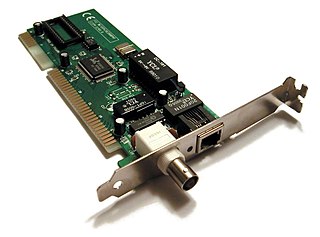
A network interface controller is a computer hardware component that connects a computer to a computer network.

Xeon is a brand of x86 microprocessors designed, manufactured, and marketed by Intel, targeted at the non-consumer workstation, server, and embedded markets. It was introduced in June 1998. Xeon processors are based on the same architecture as regular desktop-grade CPUs, but have advanced features such as support for error correction code (ECC) memory, higher core counts, more PCI Express lanes, support for larger amounts of RAM, larger cache memory and extra provision for enterprise-grade reliability, availability and serviceability (RAS) features responsible for handling hardware exceptions through the Machine Check Architecture (MCA). They are often capable of safely continuing execution where a normal processor cannot due to these extra RAS features, depending on the type and severity of the machine-check exception (MCE). Some also support multi-socket systems with two, four, or eight sockets through use of the Ultra Path Interconnect (UPI) bus, which replaced the older QuickPath Interconnect (QPI) bus.
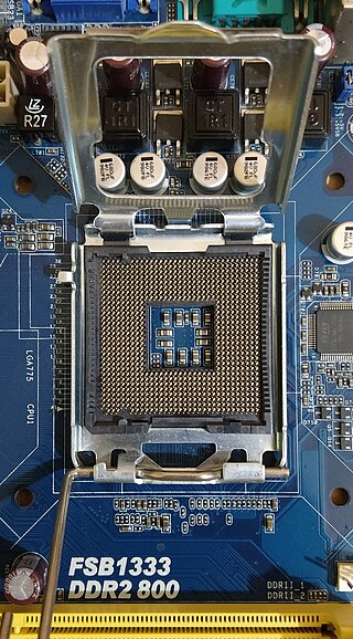
LGA 775, also known as Socket T, is an Intel desktop CPU socket. Unlike PGA CPU sockets, such as its predecessor Socket 478, LGA 775 has no socket holes; instead, it has 775 protruding pins which touch contact points on the underside of the processor (CPU).
Pentium D is a range of desktop 64-bit x86-64 processors based on the NetBurst microarchitecture, which is the dual-core variant of the Pentium 4 manufactured by Intel. Each CPU comprised two cores. The brand's first processor, codenamed Smithfield and manufactured on the 90 nm process, was released on May 25, 2005, followed by the 65 nm Presler nine months later. The core implementation on the 90 nm "Smithfield" and later 65 nm "Presler" are designed differently but are functionally the same. The 90 nm "Smithfield" contains a single die, with two adjoined but functionally separate CPU cores cut from the same wafer. The later 65 nm "Presler" utilized a multi-chip module package, where two discrete dies each containing a single core reside on the CPU substrate. Neither the 90nm "Smithfield" nor the 65 nm "Presler" were capable of direct core to core communication, relying instead on the northbridge link to send information between the 2 cores.
The Intel Core microarchitecture is a multi-core processor microarchitecture launched by Intel in mid-2006. It is a major evolution over the Yonah, the previous iteration of the P6 microarchitecture series which started in 1995 with Pentium Pro. It also replaced the NetBurst microarchitecture, which suffered from high power consumption and heat intensity due to an inefficient pipeline designed for high clock rate. In early 2004 the new version of NetBurst (Prescott) needed very high power to reach the clocks it needed for competitive performance, making it unsuitable for the shift to dual/multi-core CPUs. On May 7, 2004 Intel confirmed the cancellation of the next NetBurst, Tejas and Jayhawk. Intel had been developing Merom, the 64-bit evolution of the Pentium M, since 2001, and decided to expand it to all market segments, replacing NetBurst in desktop computers and servers. It inherited from Pentium M the choice of a short and efficient pipeline, delivering superior performance despite not reaching the high clocks of NetBurst.

Yonah is the code name of Intel's first generation 65 nm process CPU cores, based on cores of the earlier Banias / Dothan Pentium M microarchitecture. Yonah CPU cores were used within Intel's Core Solo and Core Duo mobile microprocessor products. SIMD performance on Yonah improved through the addition of SSE3 instructions and improvements to SSE and SSE2 implementations; integer performance decreased slightly due to higher latency cache. Additionally, Yonah included support for the NX bit.
Thermal Monitor 2 (TM2) is a throttling control method used on LGA 775 versions of the Core 2, Pentium Dual-Core, Pentium D, Pentium 4 and Celeron processors and also on the Pentium M series of processors. TM2 reduces processor temperature by lowering the CPU clock multiplier, and thereby the processor core speed.

In computing, Direct Media Interface (DMI) is Intel's proprietary link between the northbridge and southbridge chipset on a computer motherboard. It was first used between the 9xx chipsets and the ICH6, released in 2004. Previous Intel chipsets had used the Intel Hub Architecture to perform the same function, and server chipsets use a similar interface called Enterprise Southbridge Interface (ESI). While the "DMI" name dates back to ICH6, Intel mandates specific combinations of compatible devices, so the presence of a DMI does not guarantee by itself that a particular northbridge–southbridge combination is allowed.

The Platform Controller Hub (PCH) is a family of Intel's single-chip chipsets, first introduced in 2009. It is the successor to the Intel Hub Architecture, which used two chips–a northbridge and southbridge, and first appeared in the Intel 5 Series.

Haswell is the codename for a processor microarchitecture developed by Intel as the "fourth-generation core" successor to the Ivy Bridge. Intel officially announced CPUs based on this microarchitecture on June 4, 2013, at Computex Taipei 2013, while a working Haswell chip was demonstrated at the 2011 Intel Developer Forum. Haswell was the last generation of Intel processor to have socketed processors on mobile. With Haswell, which uses a 22 nm process, Intel also introduced low-power processors designed for convertible or "hybrid" ultrabooks, designated by the "U" suffix. Haswell began shipping to manufacturers and OEMs in mid-2013, with its desktop chips officially launched in September 2013.
Intel 5 Series is a computing architecture introduced in 2008 that improves the efficiency and balances the use of communication channels in the motherboard. The architecture consists primarily of a central processing unit (CPU) and a single chipset. All motherboard communications and activities circle around these two devices.

LGA 2011, also called Socket R, is a CPU socket by Intel released on November 14, 2011. It launched along with LGA 1356 to replace its predecessor, LGA 1366 and LGA 1567. While LGA 1356 was designed for dual-processor or low-end servers, LGA 2011 was designed for high-end desktops and high-performance servers. The socket has 2011 protruding pins that touch contact points on the underside of the processor.

Skylake is Intel's codename for its sixth generation Core microprocessor family that was launched on August 5, 2015, succeeding the Broadwell microarchitecture. Skylake is a microarchitecture redesign using the same 14 nm manufacturing process technology as its predecessor, serving as a tock in Intel's tick–tock manufacturing and design model. According to Intel, the redesign brings greater CPU and GPU performance and reduced power consumption. Skylake CPUs share their microarchitecture with Kaby Lake, Coffee Lake, Whiskey Lake, and Comet Lake CPUs.
ThinkSystem is a family of Intel servers from Lenovo. ThinkSystem products are designed to work with existing infrastructure and adapt to workloads. They are designed to provide performance, simplicity, capacity, security, and high availability for medium to large businesses. The ThinkSystem product line began with the TS100 from Lenovo.

Broadwell is the fifth generation of the Intel Core processor. It is Intel's codename for the 14 nanometer die shrink of its Haswell microarchitecture. It is a "tick" in Intel's tick–tock principle as the next step in semiconductor fabrication. Like some of the previous tick-tock iterations, Broadwell did not completely replace the full range of CPUs from the previous microarchitecture (Haswell), as there were no low-end desktop CPUs based on Broadwell.
The Intel Management Engine (ME), also known as the Intel Manageability Engine, is an autonomous subsystem that has been incorporated in virtually all of Intel's processor chipsets since 2008. It is located in the Platform Controller Hub of modern Intel motherboards.
Intel X99, codenamed "Wellsburg", is a Platform Controller Hub (PCH) designed and manufactured by Intel, targeted at the high-end desktop (HEDT) and enthusiast segments of the Intel product lineup. The X99 chipset supports both Intel Core i7 Extreme and Intel Xeon E5-16xx v3 and E5-26xx v3 processors, which belong to the Haswell-E and Haswell-EP variants of the Haswell microarchitecture, respectively. All supported processors use the LGA 2011-v3 socket.