Related Research Articles

An electric current is a flow of charged particles, such as electrons or ions, moving through an electrical conductor or space. It is defined as the net rate of flow of electric charge through a surface. The moving particles are called charge carriers, which may be one of several types of particles, depending on the conductor. In electric circuits the charge carriers are often electrons moving through a wire. In semiconductors they can be electrons or holes. In an electrolyte the charge carriers are ions, while in plasma, an ionized gas, they are ions and electrons.
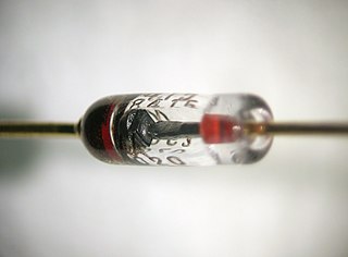
A diode is a two-terminal electronic component that conducts current primarily in one direction. It has low resistance in one direction and high resistance in the other.
A semiconductor is a material that has an electrical conductivity value falling between that of a conductor, such as copper, and an insulator, such as glass. Its resistivity generally falls as its temperature rises; metals behave in the opposite way. In many cases their conducting properties may be altered in useful ways by introducing impurities ("doping") into the crystal structure. When two differently doped regions exist in the same crystal, a semiconductor junction is created. The behavior of charge carriers, which include electrons, ions, and electron holes, at these junctions is the basis of diodes, transistors, and most modern electronics. Some examples of semiconductors are silicon, germanium, gallium arsenide, and elements near the so-called "metalloid staircase" on the periodic table. After silicon, gallium arsenide is the second-most common semiconductor and is used in laser diodes, solar cells, microwave-frequency integrated circuits, and others. Silicon is a critical element for fabricating most electronic circuits.

A transistor is a semiconductor device used to amplify or switch electrical signals and power. It is one of the basic building blocks of modern electronics. It is composed of semiconductor material, usually with at least three terminals for connection to an electronic circuit. A voltage or current applied to one pair of the transistor's terminals controls the current through another pair of terminals. Because the controlled (output) power can be higher than the controlling (input) power, a transistor can amplify a signal. Some transistors are packaged individually, but many more in miniature form are found embedded in integrated circuits. Because transistors are the key active components in practically all modern electronics, many people consider them one of the 20th century's greatest inventions.

A semiconductor device is an electronic component that relies on the electronic properties of a semiconductor material for its function. Its conductivity lies between conductors and insulators. Semiconductor devices have replaced vacuum tubes in most applications. They conduct electric current in the solid state, rather than as free electrons across a vacuum or as free electrons and ions through an ionized gas.

The metal–oxide–semiconductor field-effect transistor is a type of field-effect transistor (FET), most commonly fabricated by the controlled oxidation of silicon. It has an insulated gate, the voltage of which determines the conductivity of the device. This ability to change conductivity with the amount of applied voltage can be used for amplifying or switching electronic signals. The term metal–insulator–semiconductor field-effect transistor (MISFET) is almost synonymous with MOSFET. Another near-synonym is insulated-gate field-effect transistor (IGFET).

The junction field-effect transistor (JFET) is one of the simplest types of field-effect transistor. JFETs are three-terminal semiconductor devices that can be used as electronically controlled switches or resistors, or to build amplifiers.
A bipolar junction transistor (BJT) is a type of transistor that uses both electrons and electron holes as charge carriers. In contrast, a unipolar transistor, such as a field-effect transistor (FET), uses only one kind of charge carrier. A bipolar transistor allows a small current injected at one of its terminals to control a much larger current flowing between the terminals, making the device capable of amplification or switching.
Wide-bandgap semiconductors are semiconductor materials which have a larger band gap than conventional semiconductors. Conventional semiconductors like silicon have a bandgap in the range of 0.6 – 1.5 electronvolt (eV), whereas wide-bandgap materials have bandgaps in the range above 2 eV. Generally, wide-bandgap semiconductors have electronic properties which fall in between those of conventional semiconductors and insulators.
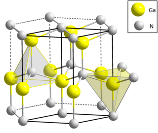
Gallium nitride is a binary III/V direct bandgap semiconductor commonly used in blue light-emitting diodes since the 1990s. The compound is a very hard material that has a Wurtzite crystal structure. Its wide band gap of 3.4 eV affords it special properties for applications in optoelectronic, high-power and high-frequency devices. For example, GaN is the substrate that makes violet (405 nm) laser diodes possible, without requiring nonlinear optical frequency doubling.
In solid-state physics, the electron mobility characterises how quickly an electron can move through a metal or semiconductor when pushed or pulled by an electric field. There is an analogous quantity for holes, called hole mobility. The term carrier mobility refers in general to both electron and hole mobility.
A power semiconductor device is a semiconductor device used as a switch or rectifier in power electronics. Such a device is also called a power device or, when used in an integrated circuit, a power IC.

A high-electron-mobility transistor, also known as heterostructure FET (HFET) or modulation-doped FET (MODFET), is a field-effect transistor incorporating a junction between two materials with different band gaps as the channel instead of a doped region. A commonly used material combination is GaAs with AlGaAs, though there is wide variation, dependent on the application of the device. Devices incorporating more indium generally show better high-frequency performance, while in recent years, gallium nitride HEMTs have attracted attention due to their high-power performance. Like other FETs, HEMTs are used in integrated circuits as digital on-off switches. FETs can also be used as amplifiers for large amounts of current using a small voltage as a control signal. Both of these uses are made possible by the FET’s unique current–voltage characteristics. HEMT transistors are able to operate at higher frequencies than ordinary transistors, up to millimeter wave frequencies, and are used in high-frequency products such as cell phones, satellite television receivers, voltage converters, and radar equipment. They are widely used in satellite receivers, in low power amplifiers and in the defense industry.

A Gunn diode, also known as a transferred electron device (TED), is a form of diode, a two-terminal semiconductor electronic component, with negative differential resistance, used in high-frequency electronics. It is based on the "Gunn effect" discovered in 1962 by physicist J. B. Gunn. Its main uses are in electronic oscillators to generate microwaves, in applications such as radar speed guns, microwave relay data link transmitters, and automatic door openers.
In semiconductor physics, the depletion region, also called depletion layer, depletion zone, junction region, space charge region, or space charge layer, is an insulating region within a conductive, doped semiconductor material where the mobile charge carriers have diffused away, or forced away by an electric field. The only elements left in the depletion region are ionized donor or acceptor impurities. This region of uncovered positive and negative ions is called the depletion region due to the depletion of carriers in this region, leaving none to carry a current. Understanding the depletion region is key to explaining modern semiconductor electronics: diodes, bipolar junction transistors, field-effect transistors, and variable capacitance diodes all rely on depletion region phenomena.
Hot carrier injection (HCI) is a phenomenon in solid-state electronic devices where an electron or a “hole” gains sufficient kinetic energy to overcome a potential barrier necessary to break an interface state. The term "hot" refers to the effective temperature used to model carrier density, not to the overall temperature of the device. Since the charge carriers can become trapped in the gate dielectric of a MOS transistor, the switching characteristics of the transistor can be permanently changed. Hot-carrier injection is one of the mechanisms that adversely affects the reliability of semiconductors of solid-state devices.
Velocity overshoot is a physical effect resulting in transit times for charge carriers between terminals that are smaller than the time required for emission of an optical phonon. The velocity therefore exceeds the saturation velocity up to three times, which leads to faster field-effect transistor or bipolar transistor switching. The effect is noticeable in the ordinary field-effect transistor for the gates shorter than 100 nm.
In solid-state physics, the Poole–Frenkel effect is a model describing the mechanism of trap-assisted electron transport in an electrical insulator. It is named after Yakov Frenkel, who published on it in 1938, extending the theory previously developed by H. H. Poole.

In physics, the field effect refers to the modulation of the electrical conductivity of a material by the application of an external electric field.

The field-effect transistor (FET) is a type of transistor that uses an electric field to control the flow of current in a semiconductor. It comes in two types: junction FET (JFET) and metal-oxide-semiconductor FET (MOSFET). FETs have three terminals: source, gate, and drain. FETs control the flow of current by the application of a voltage to the gate, which in turn alters the conductivity between the drain and source.
References
- ↑ Fundamentals of Semiconductors: Physics and Materials Properties, Peter Y. Yu, Manuel Cardona, pp. 227-228, Springer, New York 2005, ISBN 3-540-25470-6
- ↑ "Velocity Saturation" . Retrieved 2006-10-23.
- ↑ GaAs Devices and Circuits, Michael Shur, pp. 310-324, Plenum Press, NY 1987, ISBN 0-306-42192-5
- ↑ "Advanced MOSFET issues" . Retrieved 2006-10-23.
- ↑ High Field Hole Velocity and Velocity Overshoot in Silicon Inversion Layers, D. Sinitsky, F. Assaderaghi, C. Hu, and J. Bokor, IEEE Electron Device Letters, vol. 18, no. 2, February 1997