Related Research Articles

A transistor is a semiconductor device used to amplify or switch electrical signals and power. It is one of the basic building blocks of modern electronics. It is composed of semiconductor material, usually with at least three terminals for connection to an electronic circuit. A voltage or current applied to one pair of the transistor's terminals controls the current through another pair of terminals. Because the controlled (output) power can be higher than the controlling (input) power, a transistor can amplify a signal. Some transistors are packaged individually, but many more in miniature form are found embedded in integrated circuits. Because transistors are the key active components in practically all modern electronics, many people consider them one of the 20th century's greatest inventions.
Spintronics, also known as spin electronics, is the study of the intrinsic spin of the electron and its associated magnetic moment, in addition to its fundamental electronic charge, in solid-state devices. The field of spintronics concerns spin-charge coupling in metallic systems; the analogous effects in insulators fall into the field of multiferroics.
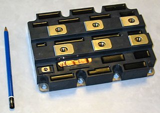
An insulated-gate bipolar transistor (IGBT) is a three-terminal power semiconductor device primarily forming an electronic switch. It was developed to combine high efficiency with fast switching. It consists of four alternating layers (P–N–P–N) that are controlled by a metal–oxide–semiconductor (MOS) gate structure.

Gallium arsenide (GaAs) is a III-V direct band gap semiconductor with a zinc blende crystal structure.
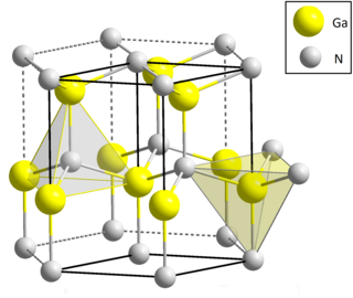
Gallium nitride is a binary III/V direct bandgap semiconductor commonly used in blue light-emitting diodes since the 1990s. The compound is a very hard material that has a Wurtzite crystal structure. Its wide band gap of 3.4 eV affords it special properties for applications in optoelectronic, high-power and high-frequency devices. For example, GaN is the substrate which makes violet (405 nm) laser diodes possible, without requiring nonlinear optical frequency-doubling.
SiGe, or silicon–germanium, is an alloy with any molar ratio of silicon and germanium, i.e. with a molecular formula of the form Si1−xGex. It is commonly used as a semiconductor material in integrated circuits (ICs) for heterojunction bipolar transistors or as a strain-inducing layer for CMOS transistors. IBM introduced the technology into mainstream manufacturing in 1989. This relatively new technology offers opportunities in mixed-signal circuit and analog circuit IC design and manufacture. SiGe is also used as a thermoelectric material for high-temperature applications (>700 K).
In solid-state physics, the electron mobility characterises how quickly an electron can move through a metal or semiconductor when pulled by an electric field. There is an analogous quantity for holes, called hole mobility. The term carrier mobility refers in general to both electron and hole mobility.
Organic semiconductors are solids whose building blocks are pi-bonded molecules or polymers made up by carbon and hydrogen atoms and – at times – heteroatoms such as nitrogen, sulfur and oxygen. They exist in the form of molecular crystals or amorphous thin films. In general, they are electrical insulators, but become semiconducting when charges are either injected from appropriate electrodes, upon doping or by photoexcitation.
Ballistic deflection transistors (BDTs) are electronic devices, developed since 2006, for high-speed integrated circuits, which is a set of circuits bounded on semiconductor material. They use electromagnetic forces instead of a logic gate, a device used to perform solely on specified inputs, to switch the forces of electrons. The unique design of this transistor includes individual electrons bouncing from wedge-shaped obstacles called deflectors. Initially accelerated by electric field, electrons are then guided on their respective paths by electromagnetic deflection. Electrons are therefore able to travel without being scattered by atoms or defects, thus resulting in improved speed and reduced power consumption.

An organic field-effect transistor (OFET) is a field-effect transistor using an organic semiconductor in its channel. OFETs can be prepared either by vacuum evaporation of small molecules, by solution-casting of polymers or small molecules, or by mechanical transfer of a peeled single-crystalline organic layer onto a substrate. These devices have been developed to realize low-cost, large-area electronic products and biodegradable electronics. OFETs have been fabricated with various device geometries. The most commonly used device geometry is bottom gate with top drain and source electrodes, because this geometry is similar to the thin-film silicon transistor (TFT) using thermally grown SiO2 as gate dielectric. Organic polymers, such as poly(methyl-methacrylate) (PMMA), can also be used as dielectric. One of the benefits of OFETs, especially compared with inorganic TFTs, is their unprecedented physical flexibility, which leads to biocompatible applications, for instance in the future health care industry of personalized biomedicines and bioelectronics.
The heterojunction bipolar transistor (HBT) is a type of bipolar junction transistor (BJT) which uses differing semiconductor materials for the emitter and base regions, creating a heterojunction. The HBT improves on the BJT in that it can handle signals of very high frequencies, up to several hundred GHz. It is commonly used in modern ultrafast circuits, mostly radio frequency (RF) systems, and in applications requiring a high power efficiency, such as RF power amplifiers in cellular phones. The idea of employing a heterojunction is as old as the conventional BJT, dating back to a patent from 1951. Detailed theory of heterojunction bipolar transistor was developed by Herbert Kroemer in 1957.
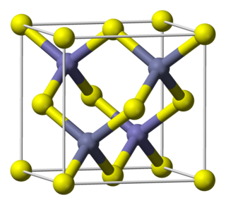
Indium antimonide (InSb) is a crystalline compound made from the elements indium (In) and antimony (Sb). It is a narrow-gap semiconductor material from the III-V group used in infrared detectors, including thermal imaging cameras, FLIR systems, infrared homing missile guidance systems, and in infrared astronomy. Indium antimonide detectors are sensitive to infrared wavelengths between 1 and 5 μm.
Ghavam G. Shahidi is an Iranian-American electrical engineer and IBM Fellow. He is the director of Silicon Technology at the IBM Thomas J Watson Research Center. He is best known for his pioneering work in silicon-on-insulator (SOI) complementary metal–oxide–semiconductor (CMOS) technology since the late 1980s.
As the devices continue to shrink further into the sub-100 nm range following the trend predicted by Moore’s law, the topic of thermal properties and transport in such nanoscale devices becomes increasingly important. Display of great potential by nanostructures for thermoelectric applications also motivates the studies of thermal transport in such devices. These fields, however, generate two contradictory demands: high thermal conductivity to deal with heating issues in sub-100 nm devices and low thermal conductivity for thermoelectric applications. These issues can be addressed with phonon engineering, once nanoscale thermal behaviors have been studied and understood.
Nanofluidic circuitry is a nanotechnology aiming for control of fluids in nanometer scale. Due to the effect of an electrical double layer within the fluid channel, the behavior of nanofluid is observed to be significantly different compared with its microfluidic counterparts. Its typical characteristic dimensions fall within the range of 1–100 nm. At least one dimension of the structure is in nanoscopic scale. Phenomena of fluids in nano-scale structure are discovered to be of different properties in electrochemistry and fluid dynamics.
Saturation velocity is the maximum velocity a charge carrier in a semiconductor, generally an electron, attains in the presence of very high electric fields. When this happens, the semiconductor is said to be in a state of velocity saturation. Charge carriers normally move at an average drift speed proportional to the electric field strength they experience temporally. The proportionality constant is known as mobility of the carrier, which is a material property. A good conductor would have a high mobility value for its charge carrier, which means higher velocity, and consequently higher current values for a given electric field strength. There is a limit though to this process and at some high field value, a charge carrier can not move any faster, having reached its saturation velocity, due to mechanisms that eventually limit the movement of the carriers in the material.
A carbon nanotube field-effect transistor (CNTFET) is a field-effect transistor that utilizes a single carbon nanotube (CNT) or an array of carbon nanotubes as the channel material, instead of bulk silicon, as in the traditional MOSFET structure. There have been major developments since CNTFETs were first demonstrated in 1998.
Mark S. Lundstrom is an American electrical engineering researcher, educator, and author. He is known for contributions to the theory, modeling, and understanding of semiconductor devices, especially nanoscale transistors, and as the creator of the nanoHUB, a major online resource for nanotechnology. Lundstrom is Don and Carol Scifres Distinguished Professor of Electrical and Computer Engineering and in 2020 served as Acting Dean of the College of Engineering at Purdue University, in West Lafayette, Indiana.

The field-effect transistor (FET) is a type of transistor that uses an electric field to control the flow of current in a semiconductor. FETs are devices with three terminals: source, gate, and drain. FETs control the flow of current by the application of a voltage to the gate, which in turn alters the conductivity between the drain and source.
References
- ↑ Jyegal, Jang (June 2015). "Velocity overshoot decay mechanisms in compound semiconductor field-effect transistors with a submicron characteristic length". AIP Advances. 5 (6): 067118. Bibcode:2015AIPA....5f7118J. doi: 10.1063/1.4922332 .
- ↑ Tan, Michael Loong Peng; Arora, Vijay K.; Saad, Ismail; Ahmadi, Mohammad Taghi; Razali, Ismail (May 2009). "The drain velocity overshoot in an 80 nm metal–oxide–semiconductor field-effect transistor". Journal of Applied Physics. 105 (7): 074503–074503–7. Bibcode:2009JAP...105g4503T. doi: 10.1063/1.3091278 . Retrieved 9 March 2018.
- ↑ SINITSKY, D.; ASSADERAGHI, F.; ORSHANSKY, M.; BOKOR, J.; HU, C. (1997). "VELOCITY OVERSHOOT OF ELECTRONS AND HOLES IN Si INVERSION LAYERS". Solid-State Electronics. 41 (8): 1119–1125. Bibcode:1997SSEle..41.1119S. CiteSeerX 10.1.1.133.2927 . doi:10.1016/S0038-1101(97)00031-2.
- ↑ Chang, M F; Ishibashi, T (1996). Current Trends In Heterojunction Bipolar Transistors. World Scientific Publishing Co. Pte. pp. 126–129. ISBN 978-981-02-2097-6.
| | This condensed matter physics-related article is a stub. You can help Wikipedia by expanding it. |