
Chemical vapor deposition (CVD) is a vacuum deposition method used to produce high-quality, and high-performance, solid materials. The process is often used in the semiconductor industry to produce thin films.
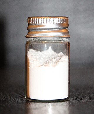
Silicon dioxide, also known as silica, is an oxide of silicon with the chemical formula SiO2, commonly found in nature as quartz. In many parts of the world, silica is the major constituent of sand. Silica is abundant as it comprises several minerals and as a synthetic products. All forms are white or colorless, although impure samples can be colored.
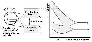
In solid-state physics and solid-state chemistry, a band gap, also called a bandgap or energy gap, is an energy range in a solid where no electronic states exist. In graphs of the electronic band structure of solids, the band gap refers to the energy difference between the top of the valence band and the bottom of the conduction band in insulators and semiconductors. It is the energy required to promote an electron from the valence band to the conduction band. The resulting conduction-band electron are free to move within the crystal lattice and serve as charge carriers to conduct electric current. It is closely related to the HOMO/LUMO gap in chemistry. If the valence band is completely full and the conduction band is completely empty, then electrons cannot move within the solid because there are no available states. If the electrons are not free to move within the crystal lattice, then there is no generated current due to no net charge carrier mobility. However, if some electrons transfer from the valence band to the conduction band, then current can flow. Therefore, the band gap is a major factor determining the electrical conductivity of a solid. Substances having large band gaps are generally insulators, those with small band gaps are semiconductor, and conductors either have very small band gaps or none, because the valence and conduction bands overlap to form a continuous band.

Gallium arsenide (GaAs) is a III-V direct band gap semiconductor with a zinc blende crystal structure.

Epitaxy refers to a type of crystal growth or material deposition in which new crystalline layers are formed with one or more well-defined orientations with respect to the crystalline seed layer. The deposited crystalline film is called an epitaxial film or epitaxial layer. The relative orientation(s) of the epitaxial layer to the seed layer is defined in terms of the orientation of the crystal lattice of each material. For most epitaxial growths, the new layer is usually crystalline and each crystallographic domain of the overlayer must have a well-defined orientation relative to the substrate crystal structure. Epitaxy can involve single-crystal structures, although grain-to-grain epitaxy has been observed in granular films. For most technological applications, single domain epitaxy, which is the growth of an overlayer crystal with one well-defined orientation with respect to the substrate crystal, is preferred. Epitaxy can also play an important role while growing superlattice structures.
Wide-bandgap semiconductors are semiconductor materials which have a larger band gap than conventional semiconductors. Conventional semiconductors like silicon have a bandgap in the range of 0.6 – 1.5 electronvolt (eV), whereas wide-bandgap materials have bandgaps in the range above 2 eV. Generally, wide-bandgap semiconductors have electronic properties which fall in between those of conventional semiconductors and insulators.
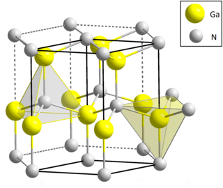
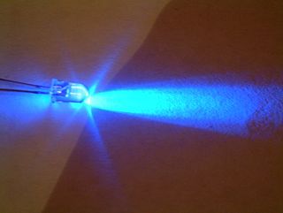
Gallium nitride is a binary III/V direct bandgap semiconductor commonly used in blue light-emitting diodes since the 1990s. The compound is a very hard material that has a Wurtzite crystal structure. Its wide band gap of 3.4 eV affords it special properties for applications in optoelectronic, high-power and high-frequency devices. For example, GaN is the substrate which makes violet (405 nm) laser diodes possible, without requiring nonlinear optical frequency-doubling.

A high-electron-mobility transistor, also known as heterostructure FET (HFET) or modulation-doped FET (MODFET), is a field-effect transistor incorporating a junction between two materials with different band gaps as the channel instead of a doped region. A commonly used material combination is GaAs with AlGaAs, though there is wide variation, dependent on the application of the device. Devices incorporating more indium generally show better high-frequency performance, while in recent years, gallium nitride HEMTs have attracted attention due to their high-power performance. Like other FETs, HEMTs are used in integrated circuits as digital on-off switches. FETs can also be used as amplifiers for large amounts of current using a small voltage as a control signal. Both of these uses are made possible by the FET’s unique current–voltage characteristics. HEMT transistors are able to operate at higher frequencies than ordinary transistors, up to millimeter wave frequencies, and are used in high-frequency products such as cell phones, satellite television receivers, voltage converters, and radar equipment. They are widely used in satellite receivers, in low power amplifiers and in the defense industry.
Aluminium nitride (AlN) is a solid nitride of aluminium. It has a high thermal conductivity of up to 321 W/(m·K) and is an electrical insulator. Its wurtzite phase (w-AlN) has a band gap of ~6 eV at room temperature and has a potential application in optoelectronics operating at deep ultraviolet frequencies.
Magnetic semiconductors are semiconductor materials that exhibit both ferromagnetism and useful semiconductor properties. If implemented in devices, these materials could provide a new type of control of conduction. Whereas traditional electronics are based on control of charge carriers, practical magnetic semiconductors would also allow control of quantum spin state. This would theoretically provide near-total spin polarization, which is an important property for spintronics applications, e.g. spin transistors.

Indium nitride is a small bandgap semiconductor material which has potential application in solar cells and high speed electronics.
In the semiconductor industry, the term high-κ dielectric refers to a material with a high dielectric constant, as compared to silicon dioxide. High-κ dielectrics are used in semiconductor manufacturing processes where they are usually used to replace a silicon dioxide gate dielectric or another dielectric layer of a device. The implementation of high-κ gate dielectrics is one of several strategies developed to allow further miniaturization of microelectronic components, colloquially referred to as extending Moore's Law. Sometimes these materials are called "high-k", instead of "high-κ".
Indium gallium nitride is a semiconductor material made of a mix of gallium nitride (GaN) and indium nitride (InN). It is a ternary group III/group V direct bandgap semiconductor. Its bandgap can be tuned by varying the amount of indium in the alloy. InxGa1−xN has a direct bandgap span from the infrared for InN to the ultraviolet of GaN. The ratio of In/Ga is usually between 0.02/0.98 and 0.3/0.7.

Hafnium(IV) oxide is the inorganic compound with the formula HfO
2. Also known as hafnium dioxide or hafnia, this colourless solid is one of the most common and stable compounds of hafnium. It is an electrical insulator with a band gap of 5.3~5.7 eV. Hafnium dioxide is an intermediate in some processes that give hafnium metal.

Indium(III) oxide (In2O3) is a chemical compound, an amphoteric oxide of indium.

I-III-VI2 semiconductors are solid semiconducting materials that contain three or more chemical elements belonging to groups I, III and VI (IUPAC groups 1/11, 13 and 16) of the periodic table. They usually involve two metals and one chalcogen. Some of these materials have a direct bandgap, Eg, of approximately 1.5 eV, which makes them efficient absorbers of sunlight and thus potential solar cell materials. A fourth element is often added to a I-III-VI2 material to tune the bandgap for maximum solar cell efficiency. A representative example is copper indium gallium selenide (CuInxGa(1–x)Se2, Eg = 1.7–1.0 eV for x = 0–1), which is used in copper indium gallium selenide solar cells.
Copper selenide is an inorganic binary compound between copper and selenium. The chemical formula depends on the ratio between the two elements, such as CuSe or Cu2Se.
Indium aluminium nitride (InAlN) is a direct bandgap semiconductor material used in the manufacture of electronic and photonic devices. It is part of the III-V group of semiconductors, being an alloy of indium nitride and aluminium nitride, and is closely related to the more widely used gallium nitride. It is of special interest in applications requiring good stability and reliability, owing to its large direct bandgap and ability to maintain operation at temperatures of up to 1000 °C., making it of particular interest to areas such as the space industry. InAlN high-electron-mobility transistors (HEMTs) are attractive candidates for such applications owing to the ability of InAlN to lattice-match to gallium nitride, eliminating a reported failure route in the closely related aluminium gallium nitride HEMTs.
Hafnium compounds are compounds containing the element hafnium (Hf). Due to the lanthanide contraction, the ionic radius of hafnium(IV) (0.78 ångström) is almost the same as that of zirconium(IV) (0.79 angstroms). Consequently, compounds of hafnium(IV) and zirconium(IV) have very similar chemical and physical properties. Hafnium and zirconium tend to occur together in nature and the similarity of their ionic radii makes their chemical separation rather difficult. Hafnium tends to form inorganic compounds in the oxidation state of +4. Halogens react with it to form hafnium tetrahalides. At higher temperatures, hafnium reacts with oxygen, nitrogen, carbon, boron, sulfur, and silicon. Some compounds of hafnium in lower oxidation states are known.

