A semiconductor is a material which has an electrical conductivity value falling between that of a conductor, such as copper, and an insulator, such as glass. Its resistivity falls as its temperature rises; metals behave in the opposite way. Its conducting properties may be altered in useful ways by introducing impurities ("doping") into the crystal structure. When two differently doped regions exist in the same crystal, a semiconductor junction is created. The behavior of charge carriers, which include electrons, ions, and electron holes, at these junctions is the basis of diodes, transistors, and most modern electronics. Some examples of semiconductors are silicon, germanium, gallium arsenide, and elements near the so-called "metalloid staircase" on the periodic table. After silicon, gallium arsenide is the second-most common semiconductor and is used in laser diodes, solar cells, microwave-frequency integrated circuits, and others. Silicon is a critical element for fabricating most electronic circuits.
Spintronics, also known as spin electronics, is the study of the intrinsic spin of the electron and its associated magnetic moment, in addition to its fundamental electronic charge, in solid-state devices. The field of spintronics concerns spin-charge coupling in metallic systems; the analogous effects in insulators fall into the field of multiferroics.
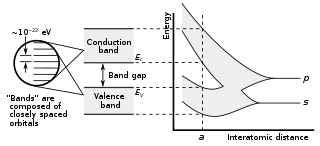
In solid-state physics and solid-state chemistry, a band gap, also called a bandgap or energy gap, is an energy range in a solid where no electronic states exist. In graphs of the electronic band structure of solids, the band gap refers to the energy difference between the top of the valence band and the bottom of the conduction band in insulators and semiconductors. It is the energy required to promote an electron from the valence band to the conduction band. The resulting conduction-band electron are free to move within the crystal lattice and serve as charge carriers to conduct electric current. It is closely related to the HOMO/LUMO gap in chemistry. If the valence band is completely full and the conduction band is completely empty, then electrons cannot move within the solid because there are no available states. If the electrons are not free to move within the crystal lattice, then there is no generated current due to no net charge carrier mobility. However, if some electrons transfer from the valence band to the conduction band, then current can flow. Therefore, the band gap is a major factor determining the electrical conductivity of a solid. Substances having large band gaps are generally insulators, those with small band gaps are semiconductor, and conductors either have very small band gaps or none, because the valence and conduction bands overlap to form a continuous band.
In solid state physics, a particle's effective mass is the mass that it seems to have when responding to forces, or the mass that it seems to have when interacting with other identical particles in a thermal distribution. One of the results from the band theory of solids is that the movement of particles in a periodic potential, over long distances larger than the lattice spacing, can be very different from their motion in a vacuum. The effective mass is a quantity that is used to simplify band structures by modeling the behavior of a free particle with that mass. For some purposes and some materials, the effective mass can be considered to be a simple constant of a material. In general, however, the value of effective mass depends on the purpose for which it is used, and can vary depending on a number of factors.

In physics, the Kondo effect describes the scattering of conduction electrons in a metal due to magnetic impurities, resulting in a characteristic change i.e. a minimum in electrical resistivity with temperature. The cause of the effect was first explained by Jun Kondo, who applied third-order perturbation theory to the problem to account for scattering of s-orbital conduction electrons off d-orbital electrons localized at impurities. Kondo's calculation predicted that the scattering rate and the resulting part of the resistivity should increase logarithmically as the temperature approaches 0 K. Experiments in the 1960s by Myriam Sarachik at Bell Laboratories provided the first data that confirmed the Kondo effect. Extended to a lattice of magnetic impurities, the Kondo effect likely explains the formation of heavy fermions and Kondo insulators in intermetallic compounds, especially those involving rare earth elements such as cerium, praseodymium, and ytterbium, and actinide elements such as uranium. The Kondo effect has also been observed in quantum dot systems.

A semimetal is a material with a very small overlap between the bottom of the conduction band and the top of the valence band. According to electronic band theory, solids can be classified as insulators, semiconductors, semimetals, or metals. In insulators and semiconductors the filled valence band is separated from an empty conduction band by a band gap. For insulators, the magnitude of the band gap is larger than that of a semiconductor. Because of the slight overlap between the conduction and valence bands, semimetals have no band gap and a negligible density of states at the Fermi level. A metal, by contrast, has an appreciable density of states at the Fermi level because the conduction band is partially filled.
In particle physics, spin polarization is the degree to which the spin, i.e., the intrinsic angular momentum of elementary particles, is aligned with a given direction. This property may pertain to the spin, hence to the magnetic moment, of conduction electrons in ferromagnetic metals, such as iron, giving rise to spin-polarized currents. It may refer to (static) spin waves, preferential correlation of spin orientation with ordered lattices.
In particle physics, a relativistic particle is an elementary particle with kinetic energy greater than or equal to its rest-mass energy given by Einstein's relation, , or specifically, of which the velocity is comparable to the speed of light .

A topological insulator is a material whose interior behaves as an electrical insulator while its surface behaves as an electrical conductor, meaning that electrons can only move along the surface of the material.

In solid-state physics, Kondo insulators (also referred as Kondo semiconductors and heavy fermion semiconductors) are understood as materials with strongly correlated electrons, that open up a narrow band gap (in the order of 10 meV) at low temperatures with the chemical potential lying in the gap, whereas in heavy fermion materials the chemical potential is located in the conduction band. The band gap opens up at low temperatures due to hybridization of localized electrons (mostly f-electrons) with conduction electrons, a correlation effect known as the Kondo effect. As a consequence, a transition from metallic behavior to insulating behavior is seen in resistivity measurements. The band gap could be either direct or indirect. Most studied Kondo insulators are FeSi, Ce3Bi4Pt3, SmB6, YbB12, and CeNiSn, although there are over a dozen known Kondo insulators.

In physics, the field effect refers to the modulation of the electrical conductivity of a material by the application of an external electric field.
Valleytronics is an experimental area in semiconductors that exploits local extrema ("valleys") in the electronic band structure. Certain semiconductors have multiple "valleys" in the electronic band structure of the first Brillouin zone, and are known as multivalley semiconductors. Valleytronics is the technology of control over the valley degree of freedom, a local maximum/minimum on the valence/conduction band, of such multivalley semiconductors.
In solid-state physics, the valence band and conduction band are the bands closest to the Fermi level, and thus determine the electrical conductivity of the solid. In nonmetals, the valence band is the highest range of electron energies in which electrons are normally present at absolute zero temperature, while the conduction band is the lowest range of vacant electronic states. On a graph of the electronic band structure of a semiconducting material, the valence band is located below the Fermi level, while the conduction band is located above it.
Bismuth antimonides, Bismuth-antimonys, or Bismuth-antimony alloys, (Bi1−xSbx) are binary alloys of bismuth and antimony in various ratios.

Dirac cones, named after Paul Dirac, are features that occur in some electronic band structures that describe unusual electron transport properties of materials like graphene and topological insulators. In these materials, at energies near the Fermi level, the valence band and conduction band take the shape of the upper and lower halves of a conical surface, meeting at what are called Dirac points.
Graphene is a semimetal whose conduction and valence bands meet at the Dirac points, which are six locations in momentum space, the vertices of its hexagonal Brillouin zone, divided into two non-equivalent sets of three points. The two sets are labeled K and K'. The sets give graphene a valley degeneracy of gv = 2. By contrast, for traditional semiconductors the primary point of interest is generally Γ, where momentum is zero. Four electronic properties separate it from other condensed matter systems.
The term Dirac matter refers to a class of condensed matter systems which can be effectively described by the Dirac equation. Even though the Dirac equation itself was formulated for fermions, the quasi-particles present within Dirac matter can be of any statistics. As a consequence, Dirac matter can be distinguished in fermionic, bosonic or anyonic Dirac matter. Prominent examples of Dirac matter are Graphene, topological insulators, Dirac semimetals, Weyl semimetals, various high-temperature superconductors with -wave pairing and liquid Helium-3. The effective theory of such systems is classified by a specific choice of the Dirac mass, the Dirac velocity, the Dirac matrices and the space-time curvature. The universal treatment of the class of Dirac matter in terms of an effective theory leads to a common features with respect to the density of states, the heat capacity and impurity scattering.
Xiaolin Wang is a Chinese-Australian scientist recognised for his work in advanced materials synthesis and characterisation and spintronics. He is director of the Institute for Superconducting and Electronic Materials, University of Wollongong. Wang is a University of Wollongong senior professor, and an Australian Research Council future fellow.

Bipolar magnetic semiconductors (BMSs) are a special class of magnetic semiconductors characterized by a unique electronic structure, where valence band maximum (VBM) and conduction band minimum (CBM) are fully spin polarized in the opposite spin direction. BMSs can be described by three energy gaps, the spin-flip gap Δ2 in valence band (VB), band gap Δ1 and spin-flip gap Δ3 in conduction band (CB). Up to now, bipolar magnetic semiconductors, together with half-metal and spin gapless semiconductor, have been viewed as three important classes of spintronic materials.

The Rashba–Edelstein effect (REE) is a spintronics-related effect, consisting in the conversion of a bidimensional charge current into a spin accumulation. This effect is an intrinsic charge-to-spin conversion mechanism and it was predicted in 1990 by the scientist V.M. Edelstein. It has been demonstrated in 2013 and confirmed by several experimental evidences in the following years.
