
An integrated circuit (IC), also known as a microchip, computer chip, or simply chip, is a small electronic device made up of multiple interconnected electronic components such as transistors, resistors, and capacitors. These components are etched onto a small piece of semiconductor material, usually silicon. Integrated circuits are used in a wide range of electronic devices, including computers, smartphones, and televisions, to perform various functions such as processing and storing information. They have greatly impacted the field of electronics by enabling device miniaturization and enhanced functionality.

Semiconductor device fabrication is the process used to manufacture semiconductor devices, typically integrated circuits (ICs) such as computer processors, microcontrollers, and memory chips. It is a multiple-step photolithographic and physio-chemical process during which electronic circuits are gradually created on a wafer, typically made of pure single-crystal semiconducting material. Silicon is almost always used, but various compound semiconductors are used for specialized applications.
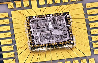
Wire bonding is a method of making interconnections between an integrated circuit (IC) or other semiconductor device and its packaging during semiconductor device fabrication. Wire bonding can also be used to connect an IC to other electronics or to connect from one printed circuit board (PCB) to another, although these are less common. Wire bonding is generally considered the most cost-effective and flexible interconnect technology and is used to assemble the vast majority of semiconductor packages. Wire bonding can be used at frequencies above 100 GHz.

Ball bonding is a type of wire bonding, and is the most common way to make the electrical interconnections between a bare silicon die and the lead frame of the package it is placed in during semiconductor device fabrication.

Flip chip, also known as controlled collapse chip connection or its abbreviation, C4, is a method for interconnecting dies such as semiconductor devices, IC chips, integrated passive devices and microelectromechanical systems (MEMS), to external circuitry with solder bumps that have been deposited onto the chip pads. The technique was developed by General Electric's Light Military Electronics Department, Utica, New York. The solder bumps are deposited on the chip pads on the top side of the wafer during the final wafer processing step. In order to mount the chip to external circuitry, it is flipped over so that its top side faces down, and aligned so that its pads align with matching pads on the external circuit, and then the solder is reflowed to complete the interconnect. This is in contrast to wire bonding, in which the chip is mounted upright and fine wires are welded onto the chip pads and lead frame contacts to interconnect the chip pads to external circuitry.

Integrated circuit packaging is the final stage of semiconductor device fabrication, in which the die is encapsulated in a supporting case that prevents physical damage and corrosion. The case, known as a "package", supports the electrical contacts which connect the device to a circuit board.

Electromigration is the transport of material caused by the gradual movement of the ions in a conductor due to the momentum transfer between conducting electrons and diffusing metal atoms. The effect is important in applications where high direct current densities are used, such as in microelectronics and related structures. As the structure size in electronics such as integrated circuits (ICs) decreases, the practical significance of this effect increases.

Ultrasonic welding is an industrial process whereby high-frequency ultrasonic acoustic vibrations are locally applied to work pieces being held together under pressure to create a solid-state weld. It is commonly used for plastics and metals, and especially for joining dissimilar materials. In ultrasonic welding, there are no connective bolts, nails, soldering materials, or adhesives necessary to bind the materials together. When used to join metals, the temperature stays well below the melting point of the involved materials, preventing any unwanted properties which may arise from high temperature exposure of the metal.

Tape-automated bonding (TAB) is a process that places bare semiconductor chips (dies) like integrated circuits onto a flexible circuit board (FPC) by attaching them to fine conductors in a polyamide or polyimide film carrier. This FPC with the die(s) can be mounted on the system or module board or assembled inside a package. Typically the FPC includes from one to three conductive layers and all inputs and outputs of the semiconductor die are connected simultaneously during the TAB bonding. Tape automated bonding is one of the methods needed for achieving chip-on-flex (COF) assembly and it is one of the first roll-to-roll processing type methods in the electronics manufacturing.

Flat no-leads packages such as quad-flat no-leads (QFN) and dual-flat no-leads (DFN) physically and electrically connect integrated circuits to printed circuit boards. Flat no-leads, also known as micro leadframe (MLF) and SON, is a surface-mount technology, one of several package technologies that connect ICs to the surfaces of PCBs without through-holes. Flat no-lead is a near chip scale plastic encapsulated package made with a planar copper lead frame substrate. Perimeter lands on the package bottom provide electrical connections to the PCB. Flat no-lead packages usually, but not always, include an exposed thermally conductive pad to improve heat transfer out of the IC. Heat transfer can be further facilitated by metal vias in the thermal pad. The QFN package is similar to the quad-flat package (QFP), and a ball grid array (BGA).
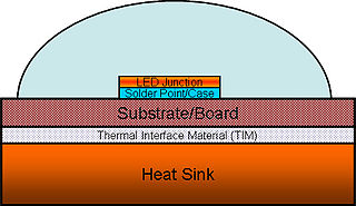
High power light-emitting diodes (LEDs) can use 350 milliwatts or more in a single LED. Most of the electricity in an LED becomes heat rather than light. If this heat is not removed, the LEDs run at high temperatures, which not only lowers their efficiency, but also makes the LED less reliable. Thus, thermal management of high power LEDs is a crucial area of research and development. It is necessary to limit both the junction and the phosphor particles temperatures to a value that will guarantee the desired LED lifetime.

Beam lead technology is a method of fabricating a semiconductor device. Its initial application was for high-frequency silicon switching transistors and high-speed integrated circuits. This technology eliminated the labor-intensive wire-bonding process that was commonly used for integrated circuits at the time. It also enabled the automated assembly of semiconductor chips onto larger substrates, facilitating the production of hybrid integrated circuits.

Thick-film technology is used to produce electronic devices/modules such as surface mount devices modules, hybrid integrated circuits, heating elements, integrated passive devices and sensors. Main manufacturing technique is screen printing (stenciling), which in addition to use in manufacturing electronic devices can also be used for various graphic reproduction targets. It became one of the key manufacturing/miniaturisation techniques of electronic devices/modules during 1950s. Typical film thickness – manufactured with thick film manufacturing processes for electronic devices – is 0.0001 to 0.1 mm.
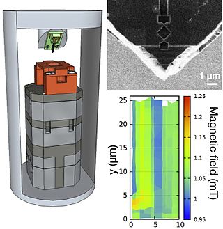
In condensed matter physics, scanning SQUID microscopy is a technique where a superconducting quantum interference device (SQUID) is used to image surface magnetic field strength with micrometre-scale resolution. A tiny SQUID is mounted onto a tip which is then rastered near the surface of the sample to be measured. As the SQUID is the most sensitive detector of magnetic fields available and can be constructed at submicrometre widths via lithography, the scanning SQUID microscope allows magnetic fields to be measured with unparalleled resolution and sensitivity. The first scanning SQUID microscope was built in 1992 by Black et al. Since then the technique has been used to confirm unconventional superconductivity in several high-temperature superconductors including YBCO and BSCCO compounds.
Thermocompression bonding describes a wafer bonding technique and is also referred to as diffusion bonding, pressure joining, thermocompression welding or solid-state welding. Two metals, e.g. gold-gold (Au), are brought into atomic contact applying force and heat simultaneously. The diffusion requires atomic contact between the surfaces due to the atomic motion. The atoms migrate from one crystal lattice to the other one based on crystal lattice vibration. This atomic interaction sticks the interface together. The diffusion process is described by the following three processes:
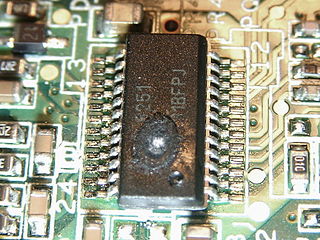
Electronic components have a wide range of failure modes. These can be classified in various ways, such as by time or cause. Failures can be caused by excess temperature, excess current or voltage, ionizing radiation, mechanical shock, stress or impact, and many other causes. In semiconductor devices, problems in the device package may cause failures due to contamination, mechanical stress of the device, or open or short circuits.
Eutectic bonding, also referred to as eutectic soldering, describes a wafer bonding technique with an intermediate metal layer that can produce a eutectic system. Those eutectic metals are alloys that transform directly from solid to liquid state, or vice versa from liquid to solid state, at a specific composition and temperature without passing a two-phase equilibrium, i.e. liquid and solid state. The fact that the eutectic temperature can be much lower than the melting temperature of the two or more pure elements can be important in eutectic bonding.

Alexander Coucoulas is an American inventor, research engineer, and author. He was named "father of thermosonic bonding" by George Harman, the world's foremost authority on wire bonding, where he referenced Coucoulas's leading edge publications in his book, Wire Bonding In Microelectronics. A thermosonic bond is formed using a set of parameters which include ultrasonic, thermal and mechanical (force) energies.

Compliant bonding is used to connect gold wires to electrical components such as integrated circuit "chips". It was invented by Alexander Coucoulas in the 1960s. The bond is formed well below the melting point of the mating gold surfaces and is therefore referred to as a solid-state type bond. The compliant bond is formed by transmitting heat and pressure to the bond region through a relatively thick indentable or compliant medium, generally an aluminum tape.
Glossary of microelectronics manufacturing terms
