
MEMS is the technology of microscopic devices incorporating both electronic and moving parts. MEMS are made up of components between 1 and 100 micrometers in size, and MEMS devices generally range in size from 20 micrometres to a millimetre, although components arranged in arrays can be more than 1000 mm2. They usually consist of a central unit that processes data and several components that interact with the surroundings.
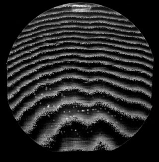
The Kirkendall effect is the motion of the interface between two metals that occurs as a consequence of the difference in diffusion rates of the metal atoms. The effect can be observed for example by placing insoluble markers at the interface between a pure metal and an alloy containing that metal, and heating to a temperature where atomic diffusion is reasonable for the given timescale; the boundary will move relative to the markers.
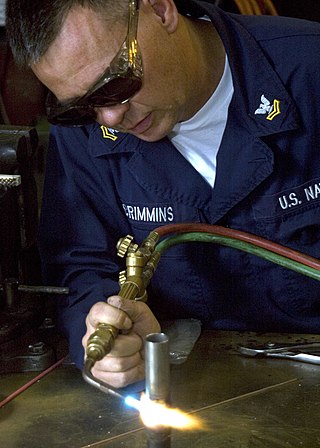
Brazing is a metal-joining process in which two or more metal items are joined together by melting and flowing a filler metal into the joint, with the filler metal having a lower melting point than the adjoining metal.
A thin film is a layer of material ranging from fractions of a nanometer (monolayer) to several micrometers in thickness. The controlled synthesis of materials as thin films is a fundamental step in many applications. A familiar example is the household mirror, which typically has a thin metal coating on the back of a sheet of glass to form a reflective interface. The process of silvering was once commonly used to produce mirrors, while more recently the metal layer is deposited using techniques such as sputtering. Advances in thin film deposition techniques during the 20th century have enabled a wide range of technological breakthroughs in areas such as magnetic recording media, electronic semiconductor devices, integrated passive devices, LEDs, optical coatings, hard coatings on cutting tools, and for both energy generation and storage. It is also being applied to pharmaceuticals, via thin-film drug delivery. A stack of thin films is called a multilayer.
Chemical mechanical polishing (CMP) or planarization is a process of smoothing surfaces with the combination of chemical and mechanical forces. It can be thought of as a hybrid of chemical etching and free abrasive polishing.
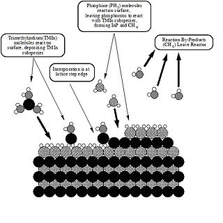
Metalorganic vapour-phase epitaxy (MOVPE), also known as organometallic vapour-phase epitaxy (OMVPE) or metalorganic chemical vapour deposition (MOCVD), is a chemical vapour deposition method used to produce single- or polycrystalline thin films. It is a process for growing crystalline layers to create complex semiconductor multilayer structures. In contrast to molecular-beam epitaxy (MBE), the growth of crystals is by chemical reaction and not physical deposition. This takes place not in vacuum, but from the gas phase at moderate pressures. As such, this technique is preferred for the formation of devices incorporating thermodynamically metastable alloys, and it has become a major process in the manufacture of optoelectronics, such as Light-emitting diodes. It was invented in 1968 at North American Aviation Science Center by Harold M. Manasevit.
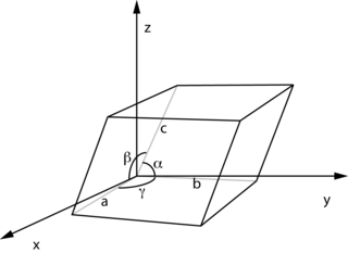
A lattice constant or lattice parameter is one of the physical dimensions and angles that determine the geometry of the unit cells in a crystal lattice, and is proportional to the distance between atoms in the crystal. A simple cubic crystal has only one lattice constant, the distance between atoms, but in general lattices in three dimensions have six lattice constants: the lengths a, b, and c of the three cell edges meeting at a vertex, and the angles α, β, and γ between those edges.
Adhesive bonding describes a wafer bonding technique with applying an intermediate layer to connect substrates of different types of materials. Those connections produced can be soluble or insoluble. The commercially available adhesive can be organic or inorganic and is deposited on one or both substrate surfaces. Adhesives, especially the well-established SU-8, and benzocyclobutene (BCB), are specialized for MEMS or electronic component production.
Thermosonic bonding is widely used to wire bond silicon integrated circuits into computers. Alexander Coucoulas was named "Father of Thermosonic Bonding" by George Harman, the world's foremost authority on wire bonding, where he referenced Coucoulas's leading edge publications in his book, Wire Bonding In Microelectronics. Owing to the well proven reliability of thermosonic bonds, it is extensively used to connect the central processing units (CPUs), which are encapsulated silicon integrated circuits that serve as the "brains" of today's computers.
Ultra-high-purity steam, also called the clean steam, UHP steam or high purity water vapor, is used in a variety of industrial manufacturing processes that require oxidation or annealing. These processes include the growth of oxide layers on silicon wafers for the semiconductor industry, originally described by the Deal-Grove model, and for the formation of passivation layers used to improve the light capture ability of crystalline photovoltaic cells. Several methods and technologies can be employed to generate ultra high purity steam, including pyrolysis, bubbling, direct liquid injection and purified steam generation. The level of purity, or the relative lack of contamination, affects the quality of the oxide layer or annealed surface. The method of delivery affects growth rate, uniformity and electrical performance. Oxidation and annealing are common steps in the manufacture of such devices as microelectronics and solar cells.
Anodic bonding is a wafer bonding process to seal glass to either silicon or metal without introducing an intermediate layer; it is commonly used to seal glass to silicon wafers in electronics and microfluidics. This bonding technique, also known as field assisted bonding or electrostatic sealing, is mostly used for connecting silicon/glass and metal/glass through electric fields. The requirements for anodic bonding are clean and even wafer surfaces and atomic contact between the bonding substrates through a sufficiently powerful electrostatic field. Also necessary is the use of borosilicate glass containing a high concentration of alkali ions. The coefficient of thermal expansion (CTE) of the processed glass needs to be similar to those of the bonding partner.
Wafer bonding is a packaging technology on wafer-level for the fabrication of microelectromechanical systems (MEMS), nanoelectromechanical systems (NEMS), microelectronics and optoelectronics, ensuring a mechanically stable and hermetically sealed encapsulation. The wafers' diameter range from 100 mm to 200 mm for MEMS/NEMS and up to 300 mm for the production of microelectronic devices. Smaller wafers were used in the early days of the microelectronics industry, with wafers being just 1 inch in diameter in the 1950s.
Eutectic bonding, also referred to as eutectic soldering, describes a wafer bonding technique with an intermediate metal layer that can produce a eutectic system. Those eutectic metals are alloys that transform directly from solid to liquid state, or vice versa from liquid to solid state, at a specific composition and temperature without passing a two-phase equilibrium, i.e. liquid and solid state. The fact that the eutectic temperature can be much lower than the melting temperature of the two or more pure elements can be important in eutectic bonding.
Glass frit bonding, also referred to as glass soldering or seal glass bonding, describes a wafer bonding technique with an intermediate glass layer. It is a widely used encapsulation technology for surface micro-machined structures, e.g., accelerometers or gyroscopes. This technique utilizes low melting-point glass and therefore provides various advantages including that viscosity of glass decreases with an increase of temperature. The viscous flow of glass has effects to compensate and planarize surface irregularities, convenient for bonding wafers with a high roughness due to plasma etching or deposition. A low viscosity promotes hermetically sealed encapsulation of structures based on a better adaption of the structured shapes. Further, the coefficient of thermal expansion (CTE) of the glass material is adapted to silicon. This results in low stress in the bonded wafer pair. The glass has to flow and wet the soldered surfaces well below the temperature where deformation or degradation of either of the joined materials or nearby structures occurs. The usual temperature of achieving flowing and wetting is between 450 and 550 °C.
Reactive bonding describes a wafer bonding procedure using highly reactive nanoscale multilayer systems as an intermediate layer between the bonding substrates. The multilayer system consists of two alternating different thin metallic films. The self-propagating exothermic reaction within the multilayer system contributes the local heat to bond the solder films. Based on the limited temperature the substrate material is exposed, temperature-sensitive components and materials with different CTEs, i.e. metals, polymers and ceramics, can be used without thermal damage.
Transient liquid phase diffusion bonding (TLPDB) is a joining process that has been applied for bonding many metallic and ceramic systems which cannot be bonded by conventional fusion welding techniques. The bonding process produces joints with a uniform composition profile, tolerant of surface oxides and geometrical defects. The bonding technique has been exploited in a wide range of applications, from the production and repair of turbine engines in the aerospace industry, to nuclear power plants, and in making connections to integrated circuit dies as a part of the microelectronics industry.

Alexander Coucoulas is an American inventor, research engineer, and author. He was named "father of thermosonic bonding" by George Harman, the world's foremost authority on wire bonding, where he referenced Coucoulas's leading edge publications in his book, Wire Bonding In Microelectronics. A thermosonic bond is formed using a set of parameters which include ultrasonic, thermal and mechanical (force) energies.

Compliant bonding is used to connect gold wires to electrical components such as integrated circuit "chips". It was invented by Alexander Coucoulas in the 1960s. The bond is formed well below the melting point of the mating gold surfaces and is therefore referred to as a solid-state type bond. The compliant bond is formed by transmitting heat and pressure to the bond region through a relatively thick indentable or compliant medium, generally an aluminum tape.
Surface activated bonding (SAB) is a low-temperature wafer bonding technology with atomically clean and activated surfaces. Surface activation prior to bonding by using fast atom bombardment is typically employed to clean the surfaces. High-strength bonding of semiconductor, metal, and dielectric can be obtained even at room temperature.
Glossary of microelectronics manufacturing terms
