Anodic bonding

Last updated

Anodic bonding is a wafer bonding process to seal glass to either silicon or metal without introducing an intermediate layer; it is commonly used to seal glass to silicon wafers in electronics and microfluidics. This bonding technique, also known as field assisted bonding or electrostatic sealing, [1] is mostly used for connecting silicon/glass and metal/glass through electric fields. The requirements for anodic bonding are clean and even wafer surfaces and atomic contact between the bonding substrates through a sufficiently powerful electrostatic field. Also necessary is the use of borosilicate glass containing a high concentration of alkali ions. The coefficient of thermal expansion (CTE) of the processed glass needs to be similar to those of the bonding partner. [2]

Contents

Anodic bonding can be applied with glass wafers at temperatures of 250 to 400 °C or with sputtered glass at 400 °C. [3] Structured borosilicate glass layers may also be deposited by plasma-assisted e-beam evaporation. [4]

This procedure is mostly used for hermetic encapsulation of micro-mechanical silicon elements. The glass substrate encapsulation protects from environmental influences, e.g. humidity or contamination. [2] Further, other materials are used for anodic bonding with silicon, i.e. low-temperature cofired ceramics (LTCC). [5]

Overview

Anodic bonding on silicon substrates is divided into bonding using a thin sheet of glass (a wafer) or a glass layer that is deposited onto the silicon using a technique such as sputtering. The glass wafer is often sodium-containing Borofloat or Pyrex glasses. With an intermediate glass layer, it is also possible to connect two silicon wafers. [6] The glass layers are deposited by sputtering, spin-on of a glass solution or vapor deposition upon the processed silicon wafer. [3] The thickness of these layers range from one to a few micrometers with spin-on glass layers needing 1 μm or less. [6] Hermetic seals of silicon to glass using an aluminum layer with thickness of 50 to 100 nm can reach strengths of 18.0 MPa. This method enables burying electrically isolated conductors in the interface. [7] Bonding of thermally oxidized wafers without a glass layer is also possible.

The procedural steps of anodic bonding are divided into the following: [2]

  1. Contact substrates
  2. Heating up substrates
  3. Bonding by the application of an electrostatic field
  4. Cooling down the wafer stack

with a process characterized by the following variables: [8]

The typical bond strength is between 10 and 20 MPa according to pull tests, higher than the fracture strength of glass.

Differing coefficients of thermal expansion pose challenges for anodic bonding. Excessive mismatch can harm the bond through intrinsic material tensions and cause disruptions in the bonding materials. The use of sodium-containing glasses, e.g. Borofloat or Pyrex, serve to reduce the mismatch. These glasses have a similar CTE to silicon in the range of applied temperature, commonly up to 400 °C. [9]

History

Anodic bonding is first mentioned by Wallis and Pomerantz in 1969. [1] It is applied as bonding of silicon wafers to sodium containing glass wafers under the influence of an applied electric field. This method is used up to date as encapsulation of sensors with electrically conducted glasses. [10]

Procedural steps of anodic bonding

Pretreatment of the substrates

The anodic bonding procedure is able to bond hydrophilic and hydrophobic silicon surfaces equally effectively. The roughness of the surface should be less than 10 nm and free of contamination on the surface for the procedure to work properly. [8] Even though anodic bonding is relatively tolerant to contaminations, a widely established cleaning procedure RCA takes place to remove any surface impurities.

The glass wafer can also be chemically etched or powder blasted for creating small cavities, where MEMS devices can be accommodated. [11]

Further mechanisms supporting the bonding process of not completely inert anodic materials can be the planarization or polishing of surfaces and the ablation of the surface layer by electrochemical etching. [8]

Contact the substrates

The wafers that meet the requirements are put into atomic contact. As soon as contact is first established, the bonding process starts close to the cathode and spreads in fronts to the edges, the process taking several minutes. [12] The anodic bonding procedure is based on a glass wafer that is usually placed above a silicon wafer. An electrode is in contact with the glass wafer either through a needle or a full area cathode electrode.

If using a needle electrode, the bond spreads radially to the outside which makes it impossible to trap air between the surfaces. The radius of the bonded area is approximately proportional to the square root of time elapsed during the procedure. Below temperatures of 350 to 400 °C and a bond voltage of 500 to 1000 V, this method is not very effective nor reliable. [13]

The use of a full area cathode electrode shows bond reactions over the whole interface after powering up the potential. [8] This is the result of a homogeneous electric field distribution at temperatures of around 300 °C and bond voltage of 250 V. [13] Using thin deposited glass layers the voltages needed can be significantly reduced. [4]

Heating and bonding by application of electrostatic field

Scheme of anodic bonding procedure. The top tool works as a cathode and the chuck as anode. B-a-schemeanodicbondprocess.png
Scheme of anodic bonding procedure. The top tool works as a cathode and the chuck as anode.
Ion drifting in bond glass influenced by electrostatic field.
(1) Formation of depletion zone (gray) through Na drifting.
(2) Drift of O ions in the depletion zone. B-a-iondriftinglass.png
Ion drifting in bond glass influenced by electrostatic field.
(1) Formation of depletion zone (gray) through Na drifting.
(2) Drift of O ions in the depletion zone.

The wafers are placed between the chuck and the top tool used as bond electrode at temperatures between 200 and 500 °C (compare to image "scheme of anodic bonding procedure") but below the softening point of glass (glass transition temperature). [11] The higher the temperature the better is the mobility of positive ions in glass.

The applied electrical potential between is set to a voltage of several 100 V. [8] This causes a diffusion of sodium ions (Na+) out of the bond interface to the backside of the glass to the cathode. That results, combined with humidity in formation of NaOH. High voltage helps to support the drifting of the positive ions in glass to the cathode. The diffusion is according to the Boltzmann distribution exponentially related to the temperature. The glass (NaO2) with its remaining oxygen ions (O2−) is negatively volume charged at the bonding surface compared to the silicon (compare to figure "ion drifting in bond glass" (1)). This is based on the depletion of Na+ ions.

Silicon is unlike, e.g. aluminium, an inert anode. In result no ions drift out of the silicon into the glass during the bond process. This affects a positive volume charge in the silicon wafer on the opposite side. [12] As a result, a few micrometer thick high-impedance depletion region is developed at the bond barrier in the glass wafer. In the gap between silicon and glass the bond voltage drops. The bond process as a combination of electrostatic and electrochemical process starts.

The electrical field intensity in the depletion region is so high that the oxygen ions drift to the bond interface and pass out to react with the silicon to form SiO2 (compare to figure "ion drifting in bond glass" (2)). Based on the high field intensity in the depletion region or in the gap at the interface, both wafer surfaces are pressed together at a specific bond voltage and bond temperature. The process is realized at temperatures from 200 - 500 °C for about 5 to 20 min. Typically, the bonding or sealing time becomes longer when temperature and voltage are reduced. [14] The pressure is applied to create intimate contact between the surfaces to ensure good electrical conduction across the wafer pair. [15] This ensures intimate contact for the surfaces of the bonding partners. The thin formed oxide layer between the bond surfaces, siloxane (Si-O-Si), ensures the irreversible connection between the bonding partners. [8]

If using thermally oxidized wafers without a glass layer, the diffusion of OH and H+ ions instead of Na+ ions leads to the bonding. [12]

Cooling down the substrate

After the bonding process, slow cooling over several minutes has to take place. This can be supported by purging with an inert gas. The cooling time depends on the difference of CTE for the bonded materials: the higher the CTE difference, the longer the cooling period.

Technical specifications

Materials
  • Si-Si
  • Si-glass
  • Si-LTCC
  • Si-glass-PZT ceramics
  • Metal-glass (Al, Cu, Kovar, Mo, Ni, Invar, ...)
Temperature
  • Si-glass: > 250 °C
  • Si-Si (w. intermediate glass layer): > 300 °C
  • Metal-glass: 200 - 450 °C
Voltage
  • Si-glass: 300 - 500 V (max. < 2000 V)
  • Metal-glass: 50 - 1500 V
Advantages
  • Easy technological processes
  • Generation of stable bonds
  • Generation of hermetic bonds
  • Bonding below 450 °C
  • Low restrictions for Si surface
Drawbacks
  • Limited allowable CTE difference in bonded materials
Research
  • Manufacturing process integration
  • Si-LTCC

Related Research Articles

<span class="mw-page-title-main">Cathode ray</span> Beam of electrons observed in vacuum tubes

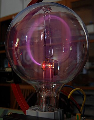
Cathode rays or electron beams (e-beam) are streams of electrons observed in discharge tubes. If an evacuated glass tube is equipped with two electrodes and a voltage is applied, glass behind the positive electrode is observed to glow, due to electrons emitted from the cathode. They were first observed in 1859 by German physicist Julius Plücker and Johann Wilhelm Hittorf, and were named in 1876 by Eugen Goldstein Kathodenstrahlen, or cathode rays. In 1897, British physicist J. J. Thomson showed that cathode rays were composed of a previously unknown negatively charged particle, which was later named the electron. Cathode-ray tubes (CRTs) use a focused beam of electrons deflected by electric or magnetic fields to render an image on a screen.

<span class="mw-page-title-main">Cathode</span> Electrode where reduction takes place

A cathode is the electrode from which a conventional current leaves a polarized electrical device. This definition can be recalled by using the mnemonic CCD for Cathode Current Departs. A conventional current describes the direction in which positive charges move. Electrons have a negative electrical charge, so the movement of electrons is opposite to that of the conventional current flow. Consequently, the mnemonic cathode current departs also means that electrons flow into the device's cathode from the external circuit. For example, the end of a household battery marked with a + (plus) is the cathode.

<span class="mw-page-title-main">Electrochemistry</span> Branch of chemistry

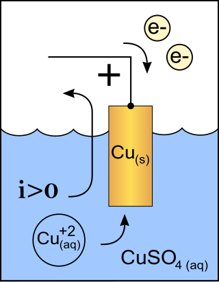
Electrochemistry is the branch of physical chemistry concerned with the relationship between electrical potential difference and identifiable chemical change. These reactions involve electrons moving via an electronically-conducting phase between electrodes separated by an ionically conducting and electronically insulating electrolyte.

<span class="mw-page-title-main">MEMS</span> Very small devices that incorporate moving components

MEMS is the technology of microscopic devices incorporating both electronic and moving parts. MEMS are made up of components between 1 and 100 micrometres in size, and MEMS devices generally range in size from 20 micrometres to a millimetre, although components arranged in arrays can be more than 1000 mm2. They usually consist of a central unit that processes data and several components that interact with the surroundings.

<span class="mw-page-title-main">Corrosion</span> Gradual destruction of materials by chemical reaction with its environment

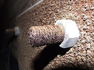
Corrosion is a natural process that converts a refined metal into a more chemically stable oxide. It is the gradual deterioration of materials by chemical or electrochemical reaction with their environment. Corrosion engineering is the field dedicated to controlling and preventing corrosion.

<span class="mw-page-title-main">Flashtube</span> Incoherent light source

A flashtube (flashlamp) is an electric arc lamp designed to produce extremely intense, incoherent, full-spectrum white light for a very short time. A flashtube is a glass tube with an electrode at each end and is filled with a gas that, when triggered, ionizes and conducts a high-voltage pulse to make light. Flashtubes are used most in photography; they also are used in science, medicine, industry, and entertainment.

<span class="mw-page-title-main">Glow discharge</span> Plasma formed by passage of current through gas

A glow discharge is a plasma formed by the passage of electric current through a gas. It is often created by applying a voltage between two electrodes in a glass tube containing a low-pressure gas. When the voltage exceeds a value called the striking voltage, the gas ionization becomes self-sustaining, and the tube glows with a colored light. The color depends on the gas used.

<span class="mw-page-title-main">Electrophoretic deposition</span>

Electrophoretic deposition (EPD), is a term for a broad range of industrial processes which includes electrocoating, cathodic electrodeposition, anodic electrodeposition, and electrophoretic coating, or electrophoretic painting. A characteristic feature of this process is that colloidal particles suspended in a liquid medium migrate under the influence of an electric field (electrophoresis) and are deposited onto an electrode. All colloidal particles that can be used to form stable suspensions and that can carry a charge can be used in electrophoretic deposition. This includes materials such as polymers, pigments, dyes, ceramics and metals.

Plasma activation is a method of surface modification employing plasma processing, which improves surface adhesion properties of many materials including metals, glass, ceramics, a broad range of polymers and textiles and even natural materials such as wood and seeds. Plasma functionalization also refers to the introduction of functional groups on the surface of exposed materials. It is widely used in industrial processes to prepare surfaces for bonding, gluing, coating and painting. Plasma processing achieves this effect through a combination of reduction of metal oxides, ultra-fine surface cleaning from organic contaminants, modification of the surface topography and deposition of functional chemical groups. Importantly, the plasma activation can be performed at atmospheric pressure using air or typical industrial gases including hydrogen, nitrogen and oxygen. Thus, the surface functionalization is achieved without expensive vacuum equipment or wet chemistry, which positively affects its costs, safety and environmental impact. Fast processing speeds further facilitate numerous industrial applications.

<span class="mw-page-title-main">Plasma-enhanced chemical vapor deposition</span> Method of depositing thin films onto a substrate

Plasma-enhanced chemical vapor deposition (PECVD) is a chemical vapor deposition process used to deposit thin films from a gas state (vapor) to a solid state on a substrate. Chemical reactions are involved in the process, which occur after creation of a plasma of the reacting gases. The plasma is generally created by radio frequency (RF) frequency or direct current (DC) discharge between two electrodes, the space between which is filled with the reacting gases.

<span class="mw-page-title-main">Radio-frequency microelectromechanical system</span>

A radio-frequency microelectromechanical system is a microelectromechanical system with electronic components comprising moving sub-millimeter-sized parts that provide radio-frequency (RF) functionality. RF functionality can be implemented using a variety of RF technologies. Besides RF MEMS technology, III-V compound semiconductor, ferrite, ferroelectric, silicon-based semiconductor, and vacuum tube technology are available to the RF designer. Each of the RF technologies offers a distinct trade-off between cost, frequency, gain, large-scale integration, lifetime, linearity, noise figure, packaging, power handling, power consumption, reliability, ruggedness, size, supply voltage, switching time and weight.

<span class="mw-page-title-main">Lithium-ion capacitor</span> Hybrid type of capacitor

A lithium-ion capacitor is a hybrid type of capacitor classified as a type of supercapacitor. It is called a hybrid because the anode is the same as those used in lithium-ion batteries and the cathode is the same as those used in supercapacitors. Activated carbon is typically used as the cathode. The anode of the LIC consists of carbon material which is often pre-doped with lithium ions. This pre-doping process lowers the potential of the anode and allows a relatively high output voltage compared to other supercapacitors.

A device generating linear or rotational motion using carbon nanotube(s) as the primary component, is termed a nanotube nanomotor. Nature already has some of the most efficient and powerful kinds of nanomotors. Some of these natural biological nanomotors have been re-engineered to serve desired purposes. However, such biological nanomotors are designed to work in specific environmental conditions. Laboratory-made nanotube nanomotors on the other hand are significantly more robust and can operate in diverse environments including varied frequency, temperature, mediums and chemical environments. The vast differences in the dominant forces and criteria between macroscale and micro/nanoscale offer new avenues to construct tailor-made nanomotors. The various beneficial properties of carbon nanotubes makes them the most attractive material to base such nanomotors on.

Direct bonding, or fusion bonding, describes a wafer bonding process without any additional intermediate layers. The bonding process is based on chemical bonds between two surfaces of any material possible meeting numerous requirements. These requirements are specified for the wafer surface as sufficiently clean, flat and smooth. Otherwise unbonded areas so called voids, i.e. interface bubbles, can occur.

Plasma-activated bonding is a derivative, directed to lower processing temperatures for direct bonding with hydrophilic surfaces. The main requirements for lowering temperatures of direct bonding are the use of materials melting at low temperatures and with different coefficients of thermal expansion (CTE).

<span class="mw-page-title-main">Eutectic bonding</span>

Eutectic bonding, also referred to as eutectic soldering, describes a wafer bonding technique with an intermediate metal layer that can produce a eutectic system. Those eutectic metals are alloys that transform directly from solid to liquid state, or vice versa from liquid to solid state, at a specific composition and temperature without passing a two-phase equilibrium, i.e. liquid and solid state. The fact that the eutectic temperature can be much lower than the melting temperature of the two or more pure elements can be important in eutectic bonding.

Glass frit bonding, also referred to as glass soldering or seal glass bonding, describes a wafer bonding technique with an intermediate glass layer. It is a widely used encapsulation technology for surface micro-machined structures, e.g., accelerometers or gyroscopes. This technique utilizes low melting-point glass and therefore provides various advantages including that viscosity of glass decreases with an increase of temperature. The viscous flow of glass has effects to compensate and planarize surface irregularities, convenient for bonding wafers with a high roughness due to plasma etching or deposition. A low viscosity promotes hermetically sealed encapsulation of structures based on a better adaption of the structured shapes. Further, the coefficient of thermal expansion (CTE) of the glass material is adapted to silicon. This results in low stress in the bonded wafer pair. The glass has to flow and wet the soldered surfaces well below the temperature where deformation or degradation of either of the joined materials or nearby structures occurs. The usual temperature of achieving flowing and wetting is between 450 and 550 °C.

Reactive bonding describes a wafer bonding procedure using highly reactive nanoscale multilayer systems as an intermediate layer between the bonding substrates. The multilayer system consists of two alternating different thin metallic films. The self-propagating exothermic reaction within the multilayer system contributes the local heat to bond the solder films. Based on the limited temperature the substrate material is exposed, temperature-sensitive components and materials with different CTEs, i.e. metals, polymers and ceramics, can be used without thermal damage.

Research in lithium-ion batteries has produced many proposed refinements of lithium-ion batteries. Areas of research interest have focused on improving energy density, safety, rate capability, cycle durability, flexibility, and cost.

<span class="mw-page-title-main">Aluminum electrolytic capacitor</span> Type of capacitor

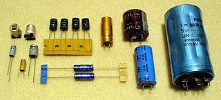
Aluminum electrolytic capacitors are (usually) polarized electrolytic capacitors whose anode electrode (+) is made of a pure aluminum foil with an etched surface. The aluminum forms a very thin insulating layer of aluminum oxide by anodization that acts as the dielectric of the capacitor. A non-solid electrolyte covers the rough surface of the oxide layer, serving in principle as the second electrode (cathode) (-) of the capacitor. A second aluminum foil called "cathode foil" contacts the electrolyte and serves as the electrical connection to the negative terminal of the capacitor.

References

  1. 1 2 Wallis, George; Pomerantz, Daniel I. (1969). "Field Assisted Glass-Metal Sealing". Journal of Applied Physics. 40 (10): 3946–3949. Bibcode:1969JAP....40.3946W. doi:10.1063/1.1657121.
  2. 1 2 3 M. Wiemer; J. Frömel; T. Gessner (2003). "Trends der Technologieentwicklung im Bereich Waferbonden". In W. Dötzel (ed.). 6. Chemnitzer Fachtagung Mikromechanik & Mikroelektronik. Vol. 6. Technische Universität Chemnitz. pp. 178–188.
  3. 1 2 Gerlach, A.; Maas, D.; Seidel, D.; Bartuch, H.; Schundau, S.; Kaschlik, K. (1999). "Low-temperature anodic bonding of silicon to silicon wafers by means of intermediate glass layers". Microsystem Technologies. 5 (3): 144–149. doi:10.1007/s005420050154. S2CID   111280889.
  4. 1 2 Leib, Juergen; Hansen, Ulli; Maus, Simon; Feindt, Holger; Hauck, Karin; Zoschke, Kai; Toepper, Michael (2010). "Anodic bonding at low voltage using microstructured borosilicate glass thin-films". 3rd Electronics System Integration Technology Conference ESTC. pp. 1–4. doi:10.1109/ESTC.2010.5642923. ISBN   978-1-4244-8553-6. S2CID   28061938.
  5. Khan, M. F.; Ghavanini, F. A.; Haasl, S.; Löfgren, L.; Persson, K.; Rusu, C.; Schjølberg-Henriksen, K.; Enoksson, P. (2010). "Methods for characterization of wafer-level encapsulation applied on silicon to LTCC anodic bonding". Journal of Micromechanics and Microengineering. 20 (6): 064020. Bibcode:2010JMiMi..20f4020K. doi:10.1088/0960-1317/20/6/064020. S2CID   111119698.
  6. 1 2 Quenzer, H. J.; Dell, C.; Wagner, B. (1996). "Silicon-silicon anodic-bonding with intermediate glass layers using spin-on glasses". Proceedings of Ninth International Workshop on Micro Electromechanical Systems. pp. 272–276. doi:10.1109/MEMSYS.1996.493993. ISBN   0-7803-2985-6. S2CID   317049.
  7. Schjølberg-Henriksen, K.; Poppe, E.; Moe, S.; Storås, P.; Taklo, M. M. V.; Wang, D. T.; Jakobsen, H. (2006). "Anodic bonding of glass to aluminium". Microsystem Technologies. 12 (5): 441–449. doi:10.1007/s00542-005-0040-8. S2CID   109085293.
  8. 1 2 3 4 5 6 7 S. Mack (1997). Eine vergleichende Untersuchung der physikalisch-chemischen Prozesse an der Grenzschicht direkt und anodischer verbundener Festkörper (Thesis). Jena, Germany: VDI Verlag / Max Planck Institute. ISBN   3-18-343602-7.
  9. T. Gessner; T. Otto; M. Wiemer; J. Frömel (2005). "Wafer bonding in micro mechanics and microelectronics - an overview". In Bernd Michel (ed.). The World of Electronic Packaging and System Integration. DDP Goldenbogen. pp. 307–313. ISBN   978-3-93243476-1.
  10. Plößl, A. (1999). "Wafer direct bonding: tailoring adhesion between brittle materials". Materials Science and Engineering. 25 (1–2): 1–88. doi:10.1016/S0927-796X(98)00017-5.
  11. 1 2 M. Chiao (2008). "Packaging (and Wire Bonding)". In D. Li (ed.). Encyclopedia of Microfluidics and Nanofluidics. Springer Science+Business Media.
  12. 1 2 3 G. Gerlach; W. Dötzel (2008). Ronald Pething (ed.). Introduction to Microsystem Technology: A Guide for Students (Wiley Microsystem and Nanotechnology). Wiley Publishing. ISBN   978-0-470-05861-9.
  13. 1 2 Nitzsche, P.; Lange, K.; Schmidt, B.; Grigull, S.; Kreissig, U.; Thomas, B.; Herzog, K. (1998). "ChemInform Abstract: Ion Drift Processes in Pyrex-Type Alkali-Borosilicate Glass During Anodic Bonding". ChemInform. 145 (5): 1755–1762. doi:10.1002/chin.199830293.
  14. Wallis, George (1975). "Field Assisted Glass Sealing". ElectroComponent Science and Technology. 2 (1): 45–53. doi: 10.1155/APEC.2.45 .
  15. S. Farrens; S. Sood (2008). "Wafer Level Packaging: Balancing Device Requirements and Materials Properties". IMAPS. International Microelectronics and Packaging Society.