An integrated circuit, also known as a microchip, chip or IC, is a small electronic device made up of multiple interconnected electronic components such as transistors, resistors, and capacitors. These components are etched onto a small piece of semiconductor material, usually silicon. Integrated circuits are used in a wide range of electronic devices, including computers, smartphones, and televisions, to perform various functions such as processing and storing information. They have greatly impacted the field of electronics by enabling device miniaturization and enhanced functionality.

MEMS is the technology of microscopic devices incorporating both electronic and moving parts. MEMS are made up of components between 1 and 100 micrometres in size, and MEMS devices generally range in size from 20 micrometres to a millimetre, although components arranged in arrays can be more than 1000 mm2. They usually consist of a central unit that processes data and several components that interact with the surroundings.
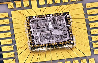
Wire bonding is a method of making interconnections between an integrated circuit (IC) or other semiconductor device and its packaging during semiconductor device fabrication. Wire bonding can also be used to connect an IC to other electronics or to connect from one printed circuit board (PCB) to another, although these are less common. Wire bonding is generally considered the most cost-effective and flexible interconnect technology and is used to assemble the vast majority of semiconductor packages. Wire bonding can be used at frequencies above 100 GHz.

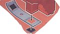
Flip chip, also known as controlled collapse chip connection or its abbreviation, C4, is a method for interconnecting dies such as semiconductor devices, IC chips, integrated passive devices and microelectromechanical systems (MEMS), to external circuitry with solder bumps that have been deposited onto the chip pads. The technique was developed by General Electric's Light Military Electronics Department, Utica, New York. The solder bumps are deposited on the chip pads on the top side of the wafer during the final wafer processing step. In order to mount the chip to external circuitry, it is flipped over so that its top side faces down, and aligned so that its pads align with matching pads on the external circuit, and then the solder is reflowed to complete the interconnect. This is in contrast to wire bonding, in which the chip is mounted upright and fine wires are welded onto the chip pads and lead frame contacts to interconnect the chip pads to external circuitry.

Integrated circuit packaging is the final stage of semiconductor device fabrication, in which the die is encapsulated in a supporting case that prevents physical damage and corrosion. The case, known as a "package", supports the electrical contacts which connect the device to a circuit board.

Diamond-like carbon (DLC) is a class of amorphous carbon material that displays some of the typical properties of diamond. DLC is usually applied as coatings to other materials that could benefit from such properties.
In electronics, a lead or pin is an electrical connector consisting of a length of wire or a metal pad that is designed to connect two locations electrically. Leads are used for many purposes, including: transfer of power; testing of an electrical circuit to see if it is working, using a test light or a multimeter; transmitting information, as when the leads from an electrocardiograph are attached to a person's body to transmit information about their heart rhythm; and sometimes to act as a heatsink. The tiny leads coming off through-hole electronic components are also often called pins; in ball grid array packages, they are in form of small spheres, and are therefore called "balls".

A system in a package (SiP) or system-in-package is a number of integrated circuits (ICs) enclosed in one chip carrier package or encompassing an IC package substrate that may include passive components and perform the functions of an entire system. The ICs may be stacked using package on package, placed side by side, and/or embedded in the substrate. The SiP performs all or most of the functions of an electronic system, and is typically used when designing components for mobile phones, digital music players, etc. Dies containing integrated circuits may be stacked vertically on the package substrate. They are internally connected by fine wires that are bonded to the package substrate. Alternatively, with a flip chip technology, solder bumps are used to join stacked chips together and to the package substrate, or even both techniques can be used in a single package. SiPs are like systems on a chip (SoCs) but less tightly integrated and not on a single semiconductor die.

Tape-automated bonding (TAB) is a process that places bare semiconductor chips (dies) like integrated circuits onto a flexible circuit board (FPC) by attaching them to fine conductors in a polyamide or polyimide film carrier. This FPC with the die(s) can be mounted on the system or module board or assembled inside a package. Typically the FPC includes from one to three conductive layers and all inputs and outputs of the semiconductor die are connected simultaneously during the TAB bonding. Tape automated bonding is one of the methods needed for achieving chip-on-flex (COF) assembly and it is one of the first roll-to-roll processing type methods in the electronics manufacturing.

Flat no-leads packages such as quad-flat no-leads (QFN) and dual-flat no-leads (DFN) physically and electrically connect integrated circuits to printed circuit boards. Flat no-leads, also known as micro leadframe (MLF) and SON, is a surface-mount technology, one of several package technologies that connect ICs to the surfaces of PCBs without through-holes. Flat no-lead is a near chip scale plastic encapsulated package made with a planar copper lead frame substrate. Perimeter lands on the package bottom provide electrical connections to the PCB. Flat no-lead packages usually, but not always, include an exposed thermally conductive pad to improve heat transfer out of the IC. Heat transfer can be further facilitated by metal vias in the thermal pad. The QFN package is similar to the quad-flat package (QFP), and a ball grid array (BGA).
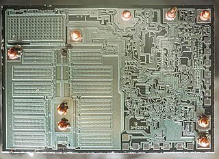
A die, in the context of integrated circuits, is a small block of semiconducting material on which a given functional circuit is fabricated. Typically, integrated circuits are produced in large batches on a single wafer of electronic-grade silicon (EGS) or other semiconductor through processes such as photolithography. The wafer is cut (diced) into many pieces, each containing one copy of the circuit. Each of these pieces is called a die.

Beam lead technology is a method of fabricating a semiconductor device. Its initial application was for high-frequency silicon switching transistors and high-speed integrated circuits. This technology eliminated the labor-intensive wire-bonding process that was commonly used for integrated circuits at the time. It also enabled the automated assembly of semiconductor chips onto larger substrates, facilitating the production of hybrid integrated circuits.

Integrated passive devices (IPDs), also known as integrated passive components (IPCs) or embedded passive components (EPC), are electronic components where resistors (R), capacitors (C), inductors (L)/coils/chokes, microstriplines, impedance matching elements, baluns or any combinations of them are integrated in the same package or on the same substrate. Sometimes integrated passives can also be called as embedded passives, and still the difference between integrated and embedded passives is technically unclear. In both cases passives are realized in between dielectric layers or on the same substrate.
A semiconductor package is a metal, plastic, glass, or ceramic casing containing one or more discrete semiconductor devices or integrated circuits. Individual components are fabricated on semiconductor wafers before being diced into die, tested, and packaged. The package provides a means for connecting it to the external environment, such as printed circuit board, via leads such as lands, balls, or pins; and protection against threats such as mechanical impact, chemical contamination, and light exposure. Additionally, it helps dissipate heat produced by the device, with or without the aid of a heat spreader. There are thousands of package types in use. Some are defined by international, national, or industry standards, while others are particular to an individual manufacturer.
Thermosonic bonding is widely used to wire bond silicon integrated circuits into computers. Alexander Coucoulas was named "Father of Thermosonic Bonding" by George Harman, the world's foremost authority on wire bonding, where he referenced Coucoulas's leading edge publications in his book, Wire Bonding In Microelectronics. Owing to the well proven reliability of thermosonic bonds, it is extensively used to connect the central processing units (CPUs), which are encapsulated silicon integrated circuits that serve as the "brains" of today's computers.
Thermocompression bonding describes a wafer bonding technique and is also referred to as diffusion bonding, pressure joining, thermocompression welding or solid-state welding. Two metals, e.g. gold-gold (Au), are brought into atomic contact applying force and heat simultaneously. The diffusion requires atomic contact between the surfaces due to the atomic motion. The atoms migrate from one crystal lattice to the other one based on crystal lattice vibration. This atomic interaction sticks the interface together. The diffusion process is described by the following three processes:
Eutectic bonding, also referred to as eutectic soldering, describes a wafer bonding technique with an intermediate metal layer that can produce a eutectic system. Those eutectic metals are alloys that transform directly from solid to liquid state, or vice versa from liquid to solid state, at a specific composition and temperature without passing a two-phase equilibrium, i.e. liquid and solid state. The fact that the eutectic temperature can be much lower than the melting temperature of the two or more pure elements can be important in eutectic bonding.

Alexander Coucoulas is an American inventor, research engineer, and author. He was named "father of thermosonic bonding" by George Harman, the world's foremost authority on wire bonding, where he referenced Coucoulas's leading edge publications in his book, Wire Bonding In Microelectronics. A thermosonic bond is formed using a set of parameters which include ultrasonic, thermal and mechanical (force) energies.

Chip on board (COB) is a method of circuit board manufacturing in which the integrated circuits (e.g. microprocessors) are attached (wired, bonded directly) to a printed circuit board, and covered by a blob of epoxy. Chip on board eliminates the packaging of individual semiconductor devices, which allows a completed product to be less costly, lighter, and more compact. In some cases, COB construction improves the operation of radio frequency systems by reducing the inductance and capacitance of integrated circuit leads.
Glossary of microelectronics manufacturing terms