Related Research Articles

An integrated circuit, also known as a microchip or IC, is a small electronic device made up of multiple interconnected electronic components such as transistors, resistors, and capacitors. These components are etched onto a small piece of semiconductor material, usually silicon. Integrated circuits are used in a wide range of electronic devices, including computers, smartphones, and televisions, to perform various functions such as processing and storing information. They have greatly impacted the field of electronics by enabling device miniaturization and enhanced functionality.

A multi-chip module (MCM) is generically an electronic assembly where multiple integrated circuits, semiconductor dies and/or other discrete components are integrated, usually onto a unifying substrate, so that in use it can be treated as if it were a larger IC. Other terms for MCM packaging include "heterogeneous integration" or "hybrid integrated circuit". The advantage of using MCM packaging is it allows a manufacturer to use multiple components for modularity and/or to improve yields over a conventional monolithic IC approach.

Integrated circuit design, or IC design, is a sub-field of electronics engineering, encompassing the particular logic and circuit design techniques required to design integrated circuits, or ICs. ICs consist of miniaturized electronic components built into an electrical network on a monolithic semiconductor substrate by photolithography.

A system in a package (SiP) or system-in-package is a number of integrated circuits (ICs) enclosed in one chip carrier package or encompassing an IC package substrate that may include passive components and perform the functions of an entire system. The ICs may be stacked using package on package, placed side by side, and/or embedded in the substrate. The SiP performs all or most of the functions of an electronic system, and is typically used when designing components for mobile phones, digital music players, etc. Dies containing integrated circuits may be stacked vertically on the package substrate. They are internally connected by fine wires that are bonded to the package substrate. Alternatively, with a flip chip technology, solder bumps are used to join stacked chips together and to the package substrate, or even both techniques can be used in a single package. SiPs are like systems on a chip (SoCs) but less tightly integrated and not on a single semiconductor die.
The transistor count is the number of transistors in an electronic device. It is the most common measure of integrated circuit complexity. The rate at which MOS transistor counts have increased generally follows Moore's law, which observes that transistor count doubles approximately every two years. However, being directly proportional to the area of a chip, transistor count does not represent how advanced the corresponding manufacturing technology is: a better indication of this is transistor density.

Multi-project chip (MPC), and multi-project wafer (MPW) semiconductor manufacturing arrangements allow customers to share tooling and microelectronics wafer fabrication cost between several designs or projects.
Package on a package (PoP) is an integrated circuit packaging method to vertically combine discrete logic and memory ball grid array (BGA) packages. Two or more packages are installed atop each other, i.e. stacked, with a standard interface to route signals between them. This allows higher component density in devices, such as mobile phones, personal digital assistants (PDA), and digital cameras, at the cost of slightly higher height requirements. Stacks with more than 2 packages are uncommon, due to heat dissipation considerations.

In electronic engineering, a through-silicon via (TSV) or through-chip via is a vertical electrical connection (via) that passes completely through a silicon wafer or die. TSVs are high-performance interconnect techniques used as an alternative to wire-bond and flip chips to create 3D packages and 3D integrated circuits. Compared to alternatives such as package-on-package, the interconnect and device density is substantially higher, and the length of the connections becomes shorter.

An interposer is an electrical interface routing between one socket or connection to another. The purpose of an interposer is to spread a connection to a wider pitch or to reroute a connection to a different connection.
A three-dimensional integrated circuit is a MOS integrated circuit (IC) manufactured by stacking as many as 16 or more ICs and interconnecting them vertically using, for instance, through-silicon vias (TSVs) or Cu-Cu connections, so that they behave as a single device to achieve performance improvements at reduced power and smaller footprint than conventional two dimensional processes. The 3D IC is one of several 3D integration schemes that exploit the z-direction to achieve electrical performance benefits in microelectronics and nanoelectronics.
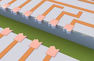
Quilt Packaging (QP) is an integrated circuit packaging and chip-to-chip interconnect packaging technology that utilizes “nodule” structures that extend out horizontally from the edges of microchips to make electrically and mechanically robust chip-to-chip interconnections.

Power management integrated circuits are integrated circuits for power management. Although PMIC refers to a wide range of chips, most include several DC/DC converters or their control part. A PMIC is often included in battery-operated devices and embedded devices to decrease the amount of space required.

Integrated passive devices (IPDs), also known as integrated passive components (IPCs) or embedded passive components (EPC), are electronic components where resistors (R), capacitors (C), inductors (L)/coils/chokes, microstriplines, impedance matching elements, baluns or any combinations of them are integrated in the same package or on the same substrate. Sometimes integrated passives can also be called as embedded passives, and still the difference between integrated and embedded passives is technically unclear. In both cases passives are realized in between dielectric layers or on the same substrate.

Wafer-level packaging (WLP) is a process where packaging components are attached to an integrated circuit (IC) before the wafer – on which the IC is fabricated – is diced. In WSP, the top and bottom layers of the packaging and the solder bumps are attached to the integrated circuits while they are still in the wafer. This process differs from a conventional process, in which the wafer is sliced into individual circuits (dice) before the packaging components are attached.
The IEEE International Electron Devices Meeting (IEDM) is an annual micro- and nanoelectronics conference held each December that serves as a forum for reporting technological breakthroughs in the areas of semiconductor and related device technologies, design, manufacturing, physics, modeling and circuit-device interaction.
High Bandwidth Memory (HBM) is a computer memory interface for 3D-stacked synchronous dynamic random-access memory (SDRAM) initially from Samsung, AMD and SK Hynix. It is used in conjunction with high-performance graphics accelerators, network devices, high-performance datacenter AI ASICs, as on-package cache in CPUs and on-package RAM in upcoming CPUs, and FPGAs and in some supercomputers. The first HBM memory chip was produced by SK Hynix in 2013, and the first devices to use HBM were the AMD Fiji GPUs in 2015.
A chiplet is a tiny integrated circuit (IC) that contains a well-defined subset of functionality. It is designed to be combined with other chiplets on an interposer in a single package. A set of chiplets can be implemented in a mix-and-match "Lego-like" assembly. This provides several advantages over a traditional system on chip (SoC):
Glossary of microelectronics manufacturing terms
Advanced packaging is the aggregation and interconnection of components before traditional integrated circuit packaging where a single die is packaged. Advanced packaging allows multiple devices to be merged and packaged as a single electronic device. Unlike traditional integrated circuit packaging, advanced packaging employs processes and techniques that are typically performed at semiconductor fabrication facilities. Advanced packaging thus sits between fabrication and traditional packaging -- or, in other terminology, between BEoL and post-fab. Advanced packaging includes multi-chip modules, 3D ICs, 2.5D ICs, heterogeneous integration, fan-out wafer-level packaging, system-in-package, quilt packaging, combining logic (processors) and memory in a single package, die stacking, several chiplets or dies in a package, combinations of these techniques, and others. 2.5D and 3D ICs are also called 2.5D or 3D packages.
Universal Chiplet Interconnect Express (UCIe) is an open specification for a die-to-die interconnect and serial bus between chiplets. It is co-developed by AMD, Arm, ASE Group, Google Cloud, Intel, Meta, Microsoft, Qualcomm, Samsung, and TSMC.
References
- ↑ "Advanced Packaging".
- ↑ "2.5D Technology". Open-silicon.com. Archived from the original on August 5, 2020. Retrieved July 21, 2020.
- 1 2 Maxfield, Max (April 8, 2012). "2D vs. 2.5D vs. 3D ICs 101". EE Times .
- ↑ Santarini, Mike (March 27, 2012). "2.5D ICs are more than a stepping stone to 3D ICs". EE Times.
- ↑ Zhang, Xiaowu; Lin, Jong Kai; Wickramanayaka, Sunil; Zhang, Songbai; Weerasekera, Roshan; Dutta, Rahul; Chang, Ka Fai; Chui, King-Jien; Li, Hong Yu; Wee Ho, David Soon; Ding, Liang; Katti, Guruprasad; Bhattacharya, Suryanarayana; Kwong, Dim-Lee (June 1, 2015). "Heterogeneous 2.5D integration on through silicon interposer". Applied Physics Reviews. 2 (2): 021308. Bibcode:2015ApPRv...2b1308Z. doi:10.1063/1.4921463 – via NASA ADS.
- ↑ "Cost and Thermal Analysis of High-Performance 2.5D and 3D Integrated Circuit Design Space" (PDF). Department of Electrical and Computer Engineering, UC Santa Barbara. 2016. Retrieved October 20, 2020.
- ↑ "Intel Custom Foundry EMIB". Intel Corporation. Archived from the original on July 13, 2015.
- ↑ "About 2.5D Technology". NHanced Semiconductors, Inc. March 23, 2017.
- ↑ "Custom ASICs". Marvell.com.
- ↑ Wong, William G. (June 6, 2016). "Q&A: A Deeper Look at Marvell's MoChi Technology". Electronicdesign.com.
- ↑ "What is SoIC?". Taiwan Semiconductor Manufacturing Company Ltd.
- ↑ "Elite Performance with AMD Ryzen 3000XT Series Processors". AMD.com. Retrieved October 20, 2020.
- ↑ "Marvell Introduces Industry's First Hyper-Scale Quad ARM Cortex-A72 and Dual Cortex-A53 Based Chips on Marvell's Revolutionary MoChi and FLC Architecture". Marvell.com. October 6, 2015.
- ↑ Moore, Samuel K. (April 12, 2019). "Intel's View of the Chiplet Revolution". IEEE Spectrum: Technology, Engineering, and Science News.
- ↑ "TSMC Announces 2x Reticle CoWoS for Next-Gen 5nm HPC Applications". 3 March 2020.