
A chemical bond is a lasting attraction between atoms or ions that enables the formation of molecules, crystals, and other structures. The bond may result from the electrostatic force between oppositely charged ions as in ionic bonds, or through the sharing of electrons as in covalent bonds. The strength of chemical bonds varies considerably; there are "strong bonds" or "primary bonds" such as covalent, ionic and metallic bonds, and "weak bonds" or "secondary bonds" such as dipole–dipole interactions, the London dispersion force, and hydrogen bonding.

A crystallographic defect is an interruption of the regular patterns of arrangement of atoms or molecules in crystalline solids. The positions and orientations of particles, which are repeating at fixed distances determined by the unit cell parameters in crystals, exhibit a periodic crystal structure, but this is usually imperfect. Several types of defects are often characterized: point defects, line defects, planar defects, bulk defects. Topological homotopy establishes a mathematical method of characterization.
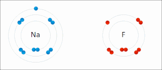
Ionic bonding is a type of chemical bonding that involves the electrostatic attraction between oppositely charged ions, or between two atoms with sharply different electronegativities, and is the primary interaction occurring in ionic compounds. It is one of the main types of bonding, along with covalent bonding and metallic bonding. Ions are atoms with an electrostatic charge. Atoms that gain electrons make negatively charged ions. Atoms that lose electrons make positively charged ions. This transfer of electrons is known as electrovalence in contrast to covalence. In the simplest case, the cation is a metal atom and the anion is a nonmetal atom, but these ions can be of a more complex nature, e.g. molecular ions like NH+
4 or SO2−
4. In simpler words, an ionic bond results from the transfer of electrons from a metal to a non-metal in order to obtain a full valence shell for both atoms.
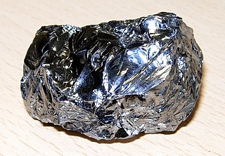
Silicon is a chemical element with the symbol Si and atomic number 14. It is a hard, brittle crystalline solid with a blue-grey metallic luster, and is a tetravalent metalloid and semiconductor. It is a member of group 14 in the periodic table: carbon is above it; and germanium, tin, lead, and flerovium are below it. It is relatively unreactive.
A semiconductor is a material which has an electrical conductivity value falling between that of a conductor, such as copper, and an insulator, such as glass. Its resistivity falls as its temperature rises; metals behave in the opposite way. Its conducting properties may be altered in useful ways by introducing impurities ("doping") into the crystal structure. When two differently doped regions exist in the same crystal, a semiconductor junction is created. The behavior of charge carriers, which include electrons, ions, and electron holes, at these junctions is the basis of diodes, transistors, and most modern electronics. Some examples of semiconductors are silicon, germanium, gallium arsenide, and elements near the so-called "metalloid staircase" on the periodic table. After silicon, gallium arsenide is the second-most common semiconductor and is used in laser diodes, solar cells, microwave-frequency integrated circuits, and others. Silicon is a critical element for fabricating most electronic circuits.

In physics, chemistry, and electronic engineering, an electron hole is a quasiparticle denoting the lack of an electron at a position where one could exist in an atom or atomic lattice. Since in a normal atom or crystal lattice the negative charge of the electrons is balanced by the positive charge of the atomic nuclei, the absence of an electron leaves a net positive charge at the hole's location.

Gallium arsenide (GaAs) is a III-V direct band gap semiconductor with a zinc blende crystal structure.

In chemistry and physics, a valence electron is an electron in the outer shell associated with an atom, and that can participate in the formation of a chemical bond if the outer shell is not closed. In a single covalent bond, a shared pair forms with both atoms in the bond each contributing one valence electron.

A p–n junction is a boundary or interface between two types of semiconductor materials, p-type and n-type, inside a single crystal of semiconductor. The "p" (positive) side contains an excess of holes, while the "n" (negative) side contains an excess of electrons in the outer shells of the electrically neutral atoms there. This allows electrical current to pass through the junction only in one direction. The p-n junction is created by doping, for example by ion implantation, diffusion of dopants, or by epitaxy. If two separate pieces of material were used, this would introduce a grain boundary between the semiconductors that would severely inhibit its utility by scattering the electrons and holes.

A high-electron-mobility transistor (HEMT), also known as heterostructure FET (HFET) or modulation-doped FET (MODFET), is a field-effect transistor incorporating a junction between two materials with different band gaps as the channel instead of a doped region. A commonly used material combination is GaAs with AlGaAs, though there is wide variation, dependent on the application of the device. Devices incorporating more indium generally show better high-frequency performance, while in recent years, gallium nitride HEMTs have attracted attention due to their high-power performance. Like other FETs, HEMTs are used in integrated circuits as digital on-off switches. FETs can also be used as amplifiers for large amounts of current using a small voltage as a control signal. Both of these uses are made possible by the FET’s unique current–voltage characteristics. HEMT transistors are able to operate at higher frequencies than ordinary transistors, up to millimeter wave frequencies, and are used in high-frequency products such as cell phones, satellite television receivers, voltage converters, and radar equipment. They are widely used in satellite receivers, in low power amplifiers and in the defense industry.
In semiconductor production, doping is the intentional introduction of impurities into an intrinsic semiconductor for the purpose of modulating its electrical, optical and structural properties. The doped material is referred to as an extrinsic semiconductor.

In chemistry, a dangling bond is an unsatisfied valence on an immobilized atom. An atom with a dangling bond is also referred to as an immobilized free radical or an immobilized radical, a reference to its structural and chemical similarity to a free radical.
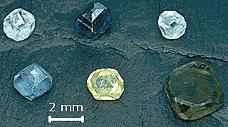
Imperfections in the crystal lattice of diamond are common. Such defects may be the result of lattice irregularities or extrinsic substitutional or interstitial impurities, introduced during or after the diamond growth. The defects affect the material properties of diamond and determine to which type a diamond is assigned; the most dramatic effects are on the diamond color and electrical conductivity, as explained by the electronic band structure.
An intrinsic (pure) semiconductor, also called an undoped semiconductor or i-type semiconductor, is a pure semiconductor without any significant dopant species present. The number of charge carriers is therefore determined by the properties of the material itself instead of the amount of impurities. In intrinsic semiconductors the number of excited electrons and the number of holes are equal: n = p. This may be the case even after doping the semiconductor, though only if it is doped with both donors and acceptors equally. In this case, n = p still holds, and the semiconductor remains intrinsic, though doped. This mean that some conductors are both intrinsic as well as extrinsic but only if n is equal to p.
An extrinsic semiconductor is one that has been doped; during manufacture of the semiconductor crystal a trace element or chemical called a doping agent has been incorporated chemically into the crystal, for the purpose of giving it different electrical properties than the pure semiconductor crystal, which is called an intrinsic semiconductor. In an extrinsic semiconductor it is these foreign dopant atoms in the crystal lattice that mainly provide the charge carriers which carry electric current through the crystal. The doping agents used are of two types, resulting in two types of extrinsic semiconductor. An electron donor dopant is an atom which, when incorporated in the crystal, releases a mobile conduction electron into the crystal lattice. An extrinsic semiconductor which has been doped with electron donor atoms is called an n-type semiconductor, because the majority of charge carriers in the crystal are negative electrons. An electron acceptor dopant is an atom which accepts an electron from the lattice, creating a vacancy where an electron should be called a hole which can move through the crystal like a positively charged particle. An extrinsic semiconductor which has been doped with electron acceptor atoms is called a p-type semiconductor, because the majority of charge carriers in the crystal are positive holes.

In semiconductor physics, a donor is a dopant atom that, when added to a semiconductor, can form a n-type region.
A dopant is a trace of impurity element that is introduced into a chemical material to alter its original electrical or optical properties. The amount of dopant necessary to cause changes is typically very low. When doped into crystalline substances, the dopant's atoms get incorporated into its crystal lattice. The crystalline materials are frequently either crystals of a semiconductor such as silicon and germanium for use in solid-state electronics, or transparent crystals for use in the production of various laser types; however, in some cases of the latter, noncrystalline substances such as glass can also be doped with impurities.
A network solid or covalent network solid is a chemical compound in which the atoms are bonded by covalent bonds in a continuous network extending throughout the material. In a network solid there are no individual molecules, and the entire crystal or amorphous solid may be considered a macromolecule. Formulas for network solids, like those for ionic compounds, are simple ratios of the component atoms represented by a formula unit.
Metals, and specifically rare-earth elements, form numerous chemical complexes with boron. Their crystal structure and chemical bonding depend strongly on the metal element M and on its atomic ratio to boron. When B/M ratio exceeds 12, boron atoms form B12 icosahedra which are linked into a three-dimensional boron framework, and the metal atoms reside in the voids of this framework. Those icosahedra are basic structural units of most allotropes of boron and boron-rich rare-earth borides. In such borides, metal atoms donate electrons to the boron polyhedra, and thus these compounds are regarded as electron-deficient solids.

Amorphous silicon (a-Si) is the non-crystalline form of silicon used for solar cells and thin-film transistors in LCDs.
