
A logic gate is an idealized or physical device that performs a Boolean function, a logical operation performed on one or more binary inputs that produces a single binary output.

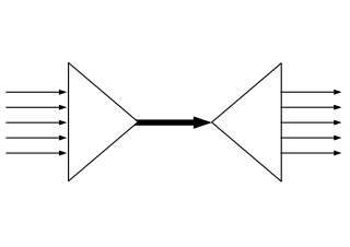
In electronics, a multiplexer, also known as a data selector, is a device that selects between several analog or digital input signals and forwards the selected input to a single output line. The selection is directed by a separate set of digital inputs known as select lines. A multiplexer of inputs has select lines, which are used to select which input line to send to the output.
Time-division multiplexing (TDM) is a method of transmitting and receiving independent signals over a common signal path by means of synchronized switches at each end of the transmission line so that each signal appears on the line only a fraction of time in an alternating pattern. It can be used when the bit rate of the transmission medium exceeds that of the signal to be transmitted. This form of signal multiplexing was developed in telecommunications for telegraphy systems in the late 19th century, but found its most common application in digital telephony in the second half of the 20th century.

In electronics and telecommunications, a crossbar switch is a collection of switches arranged in a matrix configuration. A crossbar switch has multiple input and output lines that form a crossed pattern of interconnecting lines between which a connection may be established by closing a switch located at each intersection, the elements of the matrix. Originally, a crossbar switch consisted literally of crossing metal bars that provided the input and output paths. Later implementations achieved the same switching topology in solid-state electronics. The crossbar switch is one of the principal telephone exchange architectures, together with a rotary switch, memory switch, and a crossover switch.
In electronics, a digital-to-analog converter is a system that converts a digital signal into an analog signal. An analog-to-digital converter (ADC) performs the reverse function.

A communication channel refers either to a physical transmission medium such as a wire, or to a logical connection over a multiplexed medium such as a radio channel in telecommunications and computer networking. A channel is used for information transfer of, for example, a digital bit stream, from one or several senders to one or several receivers. A channel has a certain capacity for transmitting information, often measured by its bandwidth in Hz or its data rate in bits per second.
A nonblocking minimal spanning switch is a device that can connect N inputs to N outputs in any combination. The most familiar use of switches of this type is in a telephone exchange. The term "non-blocking" means that if it is not defective, it can always make the connection. The term "minimal" means that it has the fewest possible components, and therefore the minimal expense.
In computer science, an in-place algorithm is an algorithm that operates directly on the input data structure without requiring extra space proportional to the input size. In other words, it modifies the input in place, without creating a separate copy of the data structure. An algorithm which is not in-place is sometimes called not-in-place or out-of-place.
In electronics, a crossover switch or matrix switch is a switch connecting multiple inputs to multiple outputs using complex array matrices designed to switch any one input path to any one output path(s). There are blocking and non-blocking types of cross-over switches.

An Omega network is a network configuration often used in parallel computing architectures. It is an indirect topology that relies on the perfect shuffle interconnection algorithm.

IEEE Standard 1355-1995, IEC 14575, or ISO 14575 is a data communications standard for Heterogeneous Interconnect (HIC).

A reed relay is a type of relay that uses an electromagnet to control one or more reed switches. The contacts are of magnetic material and the electromagnet acts directly on them without requiring an armature to move them. Sealed in a long, narrow glass tube, the contacts are protected from corrosion. The glass envelope may contain multiple reed switches or multiple reed switches can be inserted into a single bobbin and actuate simultaneously. Reed switches have been manufactured since the 1930s.
In the field of telecommunications, a Clos network is a kind of multistage circuit-switching network which represents a theoretical idealization of practical, multistage switching systems. It was invented by Edson Erwin in 1938 and first formalized by the American engineer Charles Clos in 1952.
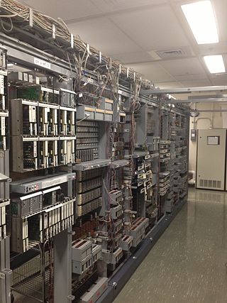
The Number One Electronic Switching System (1ESS) was the first large-scale stored program control (SPC) telephone exchange or electronic switching system in the Bell System. It was manufactured by Western Electric and first placed into service in Succasunna, New Jersey, in May 1965. The switching fabric was composed of a reed relay matrix controlled by wire spring relays which in turn were controlled by a central processing unit (CPU).
CobraNet is a combination of software, hardware, and network protocols designed to deliver uncompressed, multi-channel, low-latency digital audio over a standard Ethernet network. Developed in the 1990s, CobraNet is widely regarded as the first commercially successful audio-over-Ethernet implementation.
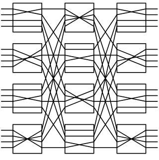
Multistage interconnection networks (MINs) are a class of high-speed computer networks usually composed of processing elements (PEs) on one end of the network and memory elements (MEs) on the other end, connected by switching elements (SEs). The switching elements themselves are usually connected to each other in stages, hence the name.
A priority encoder is a circuit or algorithm that compresses multiple binary inputs into a smaller number of outputs, similar to a simple encoder. The output of a priority encoder is the binary representation of the index of the most significant activated line. In contrast to the simple encoder, if two or more inputs to the priority encoder are active at the same time, the input having the highest priority will take precedence. It is an improvement on a simple encoder because it can handle all possible input combinations, but at the cost of extra logic.
In computing, a logic block or configurable logic block (CLB) is a fundamental building block of field-programmable gate array (FPGA) technology. Logic blocks can be configured by the engineer to provide reconfigurable logic gates.
The STC104 switch, also known as the C104 switch in its early phases, is an asynchronous packet-routing chip that was designed for building high-performance point-to-point computer communication networks. It was developed by INMOS in the 1990s and was the first example of a general-purpose production packet routing chip. It was also the first routing chip to implement wormhole routing, to decouple packet size from the flow-control protocol, and to implement interval and two-phase randomized routing.

A butterfly network is a technique to link multiple computers into a high-speed network. This form of multistage interconnection network topology can be used to connect different nodes in a multiprocessor system. The interconnect network for a shared memory multiprocessor system must have low latency and high bandwidth unlike other network systems, like local area networks (LANs) or internet for three reasons:
