Fairchild F8

Last updated
Fairchild F8
KL Fairchild F3850.jpg
F3850, the CPU of the Fairchild F8 system.
General information
Launched1975
Common manufacturer(s)
Performance
Max. CPU clock rate 1 MHz to 2 MHz
Architecture and classification
Instruction set 8-bit
Physical specifications
Package(s)

The Fairchild F8 is an 8-bit microprocessor system from Fairchild Semiconductor, announced in 1974 and shipped in 1975. [1] [2] The original processor family included four main 40-pin integrated circuits (ICs); the 3850 CPU which was the arithmetic logic unit, the 3851 Program Storage Unit (PSU) which contained 1  KB of program ROM and handled instruction decoding, and the optional 3852 Dynamic Memory Interface (DMI) or 3853 Static Memory Interface (SMI) to control additional RAM or ROM holding the user programs or data. The 3854 DMA was another optional system that added direct memory access into the RAM controlled by the 3852.

Contents

A minimal system containing a 3850 and 3851 also included four 8-bit data ports, 64 bytes of RAM, and a user program on ROM. This allowed microcontroller applications to be built using just two chips. Doing the same on more traditional designs like the Intel 8080 or Motorola 6800 normally required seven. It also meant that any application that did not fit the simple requirements generally required at least three 40-pin ICs, the CPU, PSU and either the 3852 or 3853 along with additional memory chips. As a result of these tradeoffs, the F8 series found widespread use in the microcontroller market but saw less use as a CPU in general-purpose computers. It is relatively obscure today, as its embedded uses rarely revealed the F8 inside.

In 1977, Mostek released a greatly improved single-chip implementation, the Mostek 3870. It merged the 3850 and 3851 and reduced the number of power supply voltages. More important, Mostek re-arranged the assembly line so user code in ROM was added at the last step, greatly reducing the cost of customizing the design for controller use. The 3870 replaced the original Fairchild versions and was produced by several companies in the US and Europe. In Europe, STMicroelectronics continued producing variations of the design into the mid-1990s.

History

Development

The F8 story begins with a microprocessor development project at Olympia-Werke, a subsidiary of AEG. Best known as a manufacturer of typewriters, Olympia also had a long history in mechanical calculators, a market that was rapidly converting to electronic versions. Olympia was developing a processor system known as the CP3-F, which General Instrument (GI) had licensed from them. As part of the license agreement, GI sent David Chung, head of GI's processor division, to Olympia to liaise with their design team. Shortly after returning to the US, Chung quit GI and moved to Fairchild where he became lead designer of the F8, [1] and is named as the primary inventor on the patent. [3]

Fairchild announced the F8 in September 1974, which led almost immediately to a lawsuit from GI for the misappropriation of trade secrets. As the case dragged on, in February 1976 Fairchild announced a cross-licensing deal with Olympia for the F8, meaning they now had legal access to the original CP3F design and GI's lawsuit was neutered, at least in technical details. Very little information on the CP3F is available, but it is widely believed by industry observers that the CP3F is the basis for the F8 design. [4] The court case dragged on into the 1980s, but with no technical issues of note, it had no effect on the sales of the F8. [1]

Production

The first engineering samples of the F8 were sent out in April 1975, with volume shipments beginning that fall. At the time, the electronics industry demanded second source arrangements as insurance that the design would not disappear if the designing company went bankrupt or simply lost interest in the design. Fairchild announced such an agreement with Mostek in June 1975. The agreement allowed both companies to continue independent development of the design. [1]

The F8 was introduced at a single-unit price of US$130(equivalent to $707 in 2022), making it less expensive than contemporary designs like the Intel 8080 or Motorola 6800 which were at least twice that price. Additionally, the minimal system included four 8-bit input/output ports, a small amount of RAM, and 1 KB of ROM. Together, they allowed simple applications to be built with only two ICs. In contrast, designs like the 8080 and 6800 required separate dedicated-purpose ICs to provide these functions, normally seven, [5] so an F8 system could be implemented for far less total cost. Offsetting this to some degree was that the program ROM in the PSU was masked onto the chips early in the production process, which required separate production lines for each customer. As a result, setup fees were on the order of $10,000 to 15,000. [1]

Although the F8 was marketed as a general-purpose microprocessor, historically it represents the first purpose-designed 8-bit microcontroller, [lower-alpha 1] a design that implements a complete computer system on a small number of ICs. Its release had a profound influence on the market, and led to the introduction of dedicated microcontrollers from most other vendors, among them the Intel MCS-48, Motorola MC6801 and MOS 6510, all of which combined various systems formerly left to the circuit board designer to implement. These examples, however, took the process one step further and implemented an entire system on a single IC.

Through the relentless effects of Moore's law, it was not long before the 3850 and 3851 could also be implemented in a single IC, which was released as the 3859. [1] The line was also updated with the addition of the 3856, a 3851 with 2 KB of ROM, [7] and the 3857, a 3856 with additional address lines to access external ROM in addition to the 2 KB internal, eliminating the need for a separate 3853 in many roles.

3870

Around the same time that the 3859 was released, Mostek introduced their own version of a single-chip F8, the Mostek 3870. Whereas the 3859 was essentially just a single-chip 3850/3851, the 3870 was a significant advance; it ran up to 4  MHz , double that of the 3859, and required only a single +5  V power supply instead of +5 and +12. A much more important change was that custom ROM code was now masked onto the IC as the very last step in the process, so all of the CPUs were identical until the end of the production line. As a result, the mask fees were on the order of $1,000, which made it far less expensive to implement. The 3870 was such an advance over the original that Fairchild stopped production of the 3859 and licensed the 3870 for their own sales. [1]

The 3870 was modified with many sub-versions over time. Among the most important of these was the addition of a socket on top of the chip that allowed an EPROM to be plugged in with no other support circuitry required. This eliminated the need for the on-board ROM and allowed customers to produce their own ROM and eliminate the masking fees. Variations also included examples with more ROM or RAM or other more minor changes. [1]

Meanwhile, the cross-license deal with Olympia led to production in Germany by Telefunken, another of AEG's many brands. Mostek merged with United Technologies in 1979, who drove the company into the ground and in turn, sold it to Thomson Semiconducteurs in 1985. Thomson merged with SGS in 1987 to form the modern STMicroelectronics, who continued to produce the 3870 into the 1990s. Fairchild also continued producing versions of the 3870 into the 1980s, when they were purchased by National Semiconductor. [1]

Although little-known today, "in 1977 the F8 was the world's leading microprocessor in terms of CPU sales." [8] The design remains somewhat obscure because most of those uses were as embedded microcontrollers where the chip inside the device is rarely identified, as opposed to products like home computers where the CPU inside is better known. Among its few better-known uses were the Fairchild Channel F in 1976, and in the VideoBrain Computer system in 1977. Both were wiped out of the market by the introduction of the Atari 2600 in 1977.

Fairchild also produced a number of engineering and hobby boards using the F8. Kit 1 was a single circuit board with the 3850 CPU, 3851 PSU, and 3853 SMI. The PSU contained a program known as "Fairbug" that could be accessed using a terminal connected to the CPU over its 8-bit I/O port. [9]

The F8 was discontinued in the mid-1980s, with the final last-time purchase by Innovative Data Technology, San Diego, CA for use in their flagship 1/2" 9-track tape drive the TD1050 series used for billing data interchange by telecom operators.

Description

Chip family

A typical computer system generally requires a CPU, some form of input/output to communicate with the outside world, and memory holding the program code and user data. Typically, I/O would be handled by dedicated chips, and memory would be accessed through an address bus selecting locations in external memory and then returning that data to the CPU over a data bus. Depending on the design, the I/O would communicate with the processor over a dedicated bus, or alternately by placing data in memory and then having the CPU read it. Moving data between all of these different units required additional "glue" circuitry.

The F8 was designed to split these duties up in order to make minimalistic implementations possible. [10] In theory, one could place all of these functions on a single chip, but in the era of 40-pin chips there were simply not enough pins to connect all of these functions up. In particular, implementing an 8-bit data bus, 16-bit address bus and another 8-bit I/O bus would leave only 8 more pins for every other function, from power supply and ground to the various clock signals and control lines. Other designs sometimes multiplexed the address and data lines so the same pins could be used for multiple functions, at the cost of requiring more cycles to complete an operation.

The F8 addressed this problem by internalizing some of the functions, like adding a small amount of RAM to the CPU core, while moving others out of the CPU. The best example of this is the minimal system consisting of the 3850 CPU and 3851 PSU. In this case, there is no need for an address bus at all; the RAM is contained in the 3850 and the program ROM in the 3851. It is the PSU that is responsible for keeping track of the program counter, fetching instructions from the internal ROM and feeding them to the 3850 for processing over a dedicated 5-pin instruction bus along with any associated data over the separate 8-bit data bus. [10] This freed up 11 pins that would otherwise be used for additional address lines, which, along with other simplifications and splitting of duty, allowed the CPU to have two complete I/O busses. The 3851 added another two I/O ports, so that a minimal system had four ports in total. [10]

With only 1 KB of ROM and 64 bytes of RAM, only small programs can be managed, but for many systems, like cash registers, gasoline pumps and similar roles, this is more than enough. When a system does have larger requirements, the 3852 or 3853 can be used. [11] These interface with the PSU and contain additional logic for handling their associated memory; for instance, the 3852 had a complete address bus able to access 64 KB of RAM and the circuitry needed to refresh the data. The PSU is still required in these systems, and the program counter and other pointers are maintained separately in all of these chips by reading the same control lines. The main difference between the 3852 and 3853 was that the former included the dynamic RAM refresh circuitry and a 3-pin link to the 3854 DMA controller, while the 3853 removed these and added a new interrupt handler and timer. [12]

The 3854 DMA controller was linked directly to the 3852 RAM controller and did not use the 5-pin control bus found on the other members of the family. It maintained its own address register and a separate byte count, which together indicated the block of memory to be read or written. [12]

Instruction set architecture

Fairchild F8 registers
15141312111009080706050403020100(bit position)
Main registers
 AAccumulator
Index registers
 ULISAR
DC0Data Counter 0
DC1Data Counter 1
Program counter
PC0Program Counter
PC1"Stack Pointer"
Status register
 000 I O Z C N W

Internally, the CPU contained an 8-bit accumulator, a 5-bit processor status register, a 6-bit "Indirect Scratchpad Address Register", or ISAR, and 64 bytes of "scratchpad" RAM. The first twelve locations within the RAM can be directly accessed and used as secondary accumulators, labeled A through J. The rest of the scratchpad is accessed through the ISAR, a form of indirect addressing.

The 3851/3852/3853 contain the program counter, PC0, along with a secondary program counter, PC1. PC1 was referred to as a stack pointer but was not actually used for this, it was used only to store the return addresses from subroutines and lacked any push or pop instructions. If a larger stack is required, this has to be implemented in software. These chips also had a 16-bit Data Counter, DC0, and its associated Data Counter Buffer, DC1. These were used as indexing registers for indirect addressing, although only DC0 could be accessed directly and the value in DC1 had to be swapped with DC0 using a separate instruction.

The instruction set included 70 opcodes encoded in 8-bits. As was typical of the era, many instructions had a variety of addressing modes with some of the modes encoded in the instruction opcode. For instance, the Load Register (LR) instruction came in 14 different versions depending on the origin and destination of the data. The version starting with $00 was followed by two zero bits and then another two bits indicating locations in the scratchpad in locations 12 through 15, so this used opcodes $00 through $04. $0A was another version of LR, loading the value pointed to by the ISAR. The F8 had a total of eight addressing modes. [13]

The machine instructions can be grouped into six categories: accumulator instructions, branch instructions, memory reference instructions, address register instructions, scratchpad register instruction, miscellaneous instructions (interrupt, input, output, indirect scratchpad register, load, and store). [13]

The F8 ran at 1–2  MHz , yielding a 0.5  μs cycle time. In the F8 the control bus regulates the use of the data bus through the use of timing signals and state controls. The phi clock divides the machine cycle into discrete phases depending on the instruction being executed. The five state control lines are a function of the instruction being executed. The control bus states regulate the control of information in the computer.

FAIR-BUG

The Fairchild F8 microcomputer was made available in late 1975 to electronic design engineers. The board has three large scale integration devices packaged in 40-pin ICs: CPU, PSU, and SMI. This circuit board performed as a 1 KB 8-bit personal computer which interfaced to a Teletype. The design permitted additional interfaces to floppy disk and other devices. A program called Fairbug, which resided in a 1K PSU, allowed users to view and change memory and registers, and test programs written in the machine code. This device appeared at the beginning of the transition from time shared computers to personal computers. Fairchild F8 Single-Board Microcomputer, year 1975.JPG
The Fairchild F8 microcomputer was made available in late 1975 to electronic design engineers. The board has three large scale integration devices packaged in 40-pin ICs: CPU, PSU, and SMI. This circuit board performed as a 1  KB 8-bit personal computer which interfaced to a Teletype. The design permitted additional interfaces to floppy disk and other devices. A program called Fairbug, which resided in a 1K PSU, allowed users to view and change memory and registers, and test programs written in the machine code. This device appeared at the beginning of the transition from time shared computers to personal computers.

Fairchild provided development and evaluation kits for the F8, these kits included a 3851A PSU (Program Storage Unit) which contained a monitor in mask ROM, vectored to start at address 0x8080. [14] At power-on, the ROM was entered. The ROM monitor was referred to in Fairchild literature as FAIR-BUG. [14] The FAIR-BUG monitor is a constellation of routines for assisting product development engineers who interacted with FAIR-BUG from a Teletype. Fairchild extended FAIR-BUG as KD-BUG, for use with a keyboard and display. [15]

FAIR-BUG main commands are single ASCII characters drawn from the set {A, B, C, D, E, F, G, I, L, M, N, P, R, S, W}. Register and memory locations were keyed in as parameters immediately after the command identifier. For example, the command M02F0-02FF results in the content of 16 bytes of memory being typed out by the Teletype. FAIR-BUG commands address all memory locations and all registers. These locations can be examined or modified by the programmer.

FAIR-BUG contains five subroutines which are used in processing commands: Input 2 ASCII bytes; Output 1 ASCII byte; Output the string CR, LF, Null; Output 1 ASCII byte; Input 1 ASCII byte from a Parallel Input Device. FAIR-BUG is essentially a random-access management routine for all memory, both RAM and ROM, and all registers including program counter, data counter, and scratchpad. The programmer is given the ability to plant any of the 70+ machine code instructions or operands into memory locations. The programmer can then use the G command to load a specific address into the program counter and execute the routine at that address.

The objective in providing the FAIR-BUG routines in 1975 was to assist engineers in speeding up the creation of applications for the F8 ICs.

Notes

  1. The Texas Instruments TMS 1000 pre-dates it, but is a 4-bit system. [6]

Related Research Articles

<span class="mw-page-title-main">Fairchild Channel F</span> First ROM cartridge–based video game console

The Fairchild Channel F, short for "Channel Fun", is a video game console, the first to be based on a microprocessor and to use ROM cartridges instead of having games built-in. It was released by Fairchild Camera and Instrument in November 1976 across North America at a retail price of US$169.95. It was launched as the "Video Entertainment System", but when Atari released its Video Computer System the next year, Fairchild rebranded their machine as "Channel F" while keeping the Video Entertainment System descriptor.

<span class="mw-page-title-main">Intel 8086</span> 16-bit microprocessor

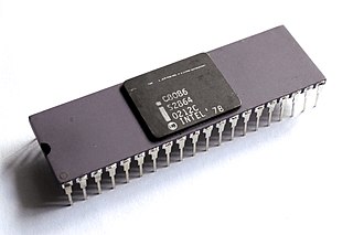
The 8086 is a 16-bit microprocessor chip designed by Intel between early 1976 and June 8, 1978, when it was released. The Intel 8088, released July 1, 1979, is a slightly modified chip with an external 8-bit data bus, and is notable as the processor used in the original IBM PC design.

<span class="mw-page-title-main">MOS Technology 6502</span> 8-bit microprocessor

The MOS Technology 6502 is an 8-bit microprocessor that was designed by a small team led by Chuck Peddle for MOS Technology. The design team had formerly worked at Motorola on the Motorola 6800 project; the 6502 is essentially a simplified, less expensive and faster version of that design.

<span class="mw-page-title-main">Motorola 6800</span> 8-bit microprocessor

The 6800 is an 8-bit microprocessor designed and first manufactured by Motorola in 1974. The MC6800 microprocessor was part of the M6800 Microcomputer System that also included serial and parallel interface ICs, RAM, ROM and other support chips. A significant design feature was that the M6800 family of ICs required only a single five-volt power supply at a time when most other microprocessors required three voltages. The M6800 Microcomputer System was announced in March 1974 and was in full production by the end of that year.

<span class="mw-page-title-main">Zilog Z80</span> 8-bit microprocessor

The Z80 is an 8-bit microprocessor introduced by Zilog as the startup company's first product. The Z80 was conceived by Federico Faggin in late 1974 and developed by him and his 11 employees starting in early 1975. The first working samples were delivered in March 1976, and it was officially introduced on the market in July 1976. With the revenue from the Z80, the company built its own chip factories and grew to over a thousand employees over the following two years.

The NS32000, sometimes known as the 32k, is a series of microprocessors produced by National Semiconductor. The first member of the family came to market in 1982, briefly known as the 16032 before becoming the 32016. It was the first general-purpose microprocessor on the market that used 32-bit data throughout: the Motorola 68000 used 32-bit data but had a 16-bit ALU and thus took twice as long perform many operations. However, the 32016 contained many bugs and often could not be run at its rated speed. These problems, and the presence of the otherwise similar 68000 which had been available since 1980, led to little use in the market.

In computer architecture, 8-bit integers or other data units are those that are 8 bits wide. Also, 8-bit central processing unit (CPU) and arithmetic logic unit (ALU) architectures are those that are based on registers or data buses of that size. Memory addresses for 8-bit CPUs are generally larger than 8-bit, usually 16-bit. 8-bit microcomputers are microcomputers that use 8-bit microprocessors.

<span class="mw-page-title-main">Intel 8085</span> 8-bit microprocessor by Intel

The Intel 8085 ("eighty-eighty-five") is an 8-bit microprocessor produced by Intel and introduced in March 1976. It is software-binary compatible with the more-famous Intel 8080 with only two minor instructions added to support its added interrupt and serial input/output features. However, it requires less support circuitry, allowing simpler and less expensive microcomputer systems to be built. The "5" in the part number highlighted the fact that the 8085 uses a single +5-volt (V) power supply by using depletion-mode transistors, rather than requiring the +5 V, −5 V and +12 V supplies needed by the 8080. This capability matched that of the competing Z80, a popular 8080-derived CPU introduced the year before. These processors could be used in computers running the CP/M operating system.

<span class="mw-page-title-main">Intel 4004</span> 4-bit microprocessor

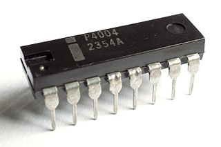
The Intel 4004 is a 4-bit central processing unit (CPU) released by Intel Corporation in 1971. Sold for US$60, it was the first commercially produced microprocessor, and the first in a long line of Intel CPUs.

<span class="mw-page-title-main">Intel 4040</span> 4-bit microprocessor introduced in 1974 by Intel

The Intel 4040 microprocessor was the successor to the Intel 4004, introduced in 1974. The 4040 employed a 10 μm silicon gate enhancement-load PMOS technology, was made up of 3,000 transistors and could execute approximately 62,000 instructions per second.

The National Semiconductor COP8 is an 8-bit CISC core microcontroller. COP8 is an enhancement to the earlier COP400 4-bit microcontroller family. COP8 main features are:

The TMS9900 was one of the first commercially available, single-chip 16-bit microprocessors. Introduced in June 1976, it implemented Texas Instruments' TI-990 minicomputer architecture in a single-chip format, and was initially used for low-end models of that lineup.

<span class="mw-page-title-main">Mostek</span> American electronics company

Mostek Corporation was a semiconductor integrated circuit manufacturer, founded in 1969 by L. J. Sevin, Louay E. Sharif, Richard L. Petritz and other ex-employees of Texas Instruments. At its peak in the late 1970s, Mostek held an 85% market share of the dynamic random-access memory (DRAM) memory chip market worldwide, until being eclipsed by lower-priced Japanese DRAM manufacturers who were accused of dumping memory on the market.

<span class="mw-page-title-main">National Semiconductor SC/MP</span> 8-bit microprocessor

National Semiconductor's SC/MP for Simple Cost-effective Micro Processor, is an early 8-bit microprocessor which became available in April 1976. It was designed to allow systems to be implemented with the minimum number of additional support chips. SC/MP included a daisy-chained control pin that allowed up to three SC/MP's share a single main memory to produce a multiprocessor system, or to act as controllers in a system with another main central processing unit (CPU). Three versions were released over its lifetime, SCMP-1 through 3, the latter two also known as INS8060 and INS8070.

<span class="mw-page-title-main">Signetics 2650</span> 8-bit microprocessor

The Signetics 2650 was an 8-bit microprocessor introduced in July 1975. According to Adam Osborne's book An Introduction to Microprocessors Vol 2: Some Real Products, it was "the most minicomputer-like" of the microprocessors available at the time. A combination of missing features and odd memory access limited its appeal, and the system saw little use in the market.

Scratchpad memory (SPM), also known as scratchpad, scratchpad RAM or local store in computer terminology, is an internal memory, usually high-speed, used for temporary storage of calculations, data, and other work in progress. In reference to a microprocessor, scratchpad refers to a special high-speed memory used to hold small items of data for rapid retrieval. It is similar to the usage and size of a scratchpad in life: a pad of paper for preliminary notes or sketches or writings, etc. When the scratchpad is a hidden portion of the main memory then it is sometimes referred to as bump storage.

<span class="mw-page-title-main">Electronic Arrays 9002</span> 1976 microprocessor

The Electronic Arrays 9002, or EA9002, was an 8-bit microprocessor released in 1976. It was designed to be easy to implement in systems with few required support chips. It included 64 bytes of built-in RAM and could be directly connected to TTL devices. It was packaged in a 28-pin DIP which made it less expensive to implement than contemporary designs like the 40-pin MOS 6502 and Zilog Z80. Today it would be known as a microcontroller, although that term did not exist at the time.

The Mostek MK5065 was an 8-bit microprocessor introduced by Mostek in early 1974. The design was originally developed by Motorola for use in an Olivetti electronic calculator, and was licensed to Mostek for use in non-calculator roles. It featured three sets of processor registers, allowing it to switch to an interrupt handler in a single cycle, and a wait-for-data mode that aided direct memory access.

<span class="mw-page-title-main">COP400</span> 4-bit microcontroller family

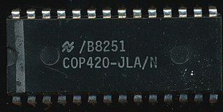
The COP400 or COP II is a 4-bit microcontroller family introduced in 1977 by National Semiconductor as a follow-on product to their original PMOS COP microcontroller. COP400 family members are complete microcomputers containing internal timing, logic, ROM, RAM, and I/O necessary to implement dedicated controllers. Some COP400 devices were second-sourced by Western Digital as the WD4200 family. In the Soviet Union several COP400 microcontrollers were manufactured as the 1820 series.

<span class="mw-page-title-main">Rockwell PPS-4</span> 4-bit microprocessor

The Rockwell PPS-4, short for "Parallel Processing System, 4-bit", was an early 4-bit microprocessor from Rockwell International, released in late 1972. Although practically unknown today, the PPS series was widely used in calculators, games and toys, and other embedded applications. Updated versions continued to be produced into the 1980s.

References

Citations

  1. 1 2 3 4 5 6 7 8 9 CPU 2013.
  2. "The Fairchild F8". The Antique Chip Collector's Page. Retrieved August 18, 2013.
  3. USPatent 3984813, assigned to Fairchild Camera and Instrument Corporation
  4. Singer, Graham (1 October 2020). "The History of the Microprocessor and the Personal Computer". Techspot.
  5. Osborne 1978, p. 2.1.
  6. Osborne 1978, p. 1.1.
  7. F3851/F3856 Program Storage Unit (PDF) (Technical report).
  8. "8-bit Microprocessors - F8 (3850)". Archived from the original on July 17, 2011. Retrieved 2013-08-18.
  9. The One-Card F8 Microprocessor Evaluation System Instruction Sheet, Fairchild Microsystems, February 13, 1976.
  10. 1 2 3 F8 1975, p. 1.
  11. F8 1975, p. 5.
  12. 1 2 F8 1975, p. 3.
  13. 1 2 F8 1975, p. 8.
  14. 1 2 F8 Microprocessor Development Support Hardware (PDF). Fairchild Semiconductor.
  15. KD-BUG User's Guide (PDF). Fairchild Semiconductor. 1978.

Bibliography