A diode is a two-terminal electronic component that conducts current primarily in one direction ; it has low resistance in one direction, and high resistance in the other.
Photocurrent is the electric current through a photosensitive device, such as a photodiode, as the result of exposure to radiant power. The photocurrent may occur as a result of the photoelectric, photoemissive, or photovoltaic effect. The photocurrent may be enhanced by internal gain caused by interaction among ions and photons under the influence of applied fields, such as occurs in an avalanche photodiode (APD).
A PIN diode is a diode with a wide, undoped intrinsic semiconductor region between a p-type semiconductor and an n-type semiconductor region. The p-type and n-type regions are typically heavily doped because they are used for ohmic contacts.
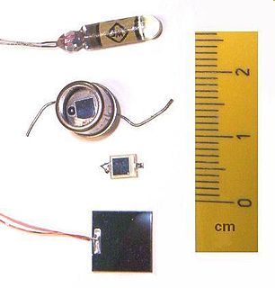
A photodiode is a semiconductor p–n junction device that converts light into an electrical current. The current is generated when photons are absorbed in the photodiode. Photodiodes may contain optical filters, built-in lenses, and may have large or small surface areas. Photodiodes usually have a slower response time as their surface area increases. The common, traditional solar cell used to generate electric solar power is a large area photodiode.

A photoresistor is a passive component that decreases resistance with respect to receiving luminosity (light) on the component's sensitive surface. The resistance of a photoresistor decreases with increase in incident l intensity; in other words, it exhibits photoconductivity. A photoresistor can be applied in light-sensitive detector circuits and light-activated and dark-activated switching circuits acting as a resistance semiconductor. In the dark, a photoresistor can have a resistance as high as several megaohms (MΩ), while in the light, a photoresistor can have a resistance as low as a few hundred ohms. If incident light on a photoresistor exceeds a certain frequency, photons absorbed by the semiconductor give bound electrons enough energy to jump into the conduction band. The resulting free electrons conduct electricity, thereby lowering resistance. The resistance range and sensitivity of a photoresistor can substantially differ among dissimilar devices. Moreover, unique photoresistors may react substantially differently to photons within certain wavelength bands.

Photomultiplier tubes (photomultipliers or PMTs for short), members of the class of vacuum tubes, and more specifically vacuum phototubes, are extremely sensitive detectors of light in the ultraviolet, visible, and near-infrared ranges of the electromagnetic spectrum. These detectors multiply the current produced by incident light by as much as 100 million times or 108 (i.e., 160 dB), in multiple dynode stages, enabling (for example) individual photons to be detected when the incident flux of light is low.
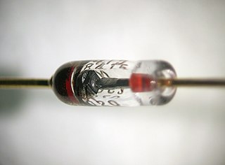
In electronics, an avalanche diode is a diode that is designed to experience avalanche breakdown at a specified reverse bias voltage. The junction of an avalanche diode is designed to prevent current concentration and resulting hot spots, so that the diode is undamaged by the breakdown. The avalanche breakdown is due to minority carriers accelerated enough to create ionization in the crystal lattice, producing more carriers, which in turn create more ionization. Because the avalanche breakdown is uniform across the whole junction, the breakdown voltage is nearly constant with changing current when compared to a non-avalanche diode.

An avalanche photodiode (APD) is a highly sensitive semiconductor photodiode detector that exploits the photoelectric effect to convert light into electricity. From a functional standpoint, they can be regarded as the semiconductor analog of photomultiplier tubes. The avalanche photodiode (APD) was invented by Japanese engineer Jun-ichi Nishizawa in 1952. However, study of avalanche breakdown, microplasma defects in Silicon and Germanium and the investigation of optical detection using p-n junctions predate this patent. Typical applications for APDs are laser rangefinders, long-range fiber-optic telecommunication, and quantum sensing for control algorithms. New applications include positron emission tomography and particle physics. APD arrays are becoming commercially available, also lightning detection and optical SETI may be future applications. It has been discovered in 2020 that adding graphene layer can prevent degradation over time to keep avalanche photodiodes like new, which is important in shrinking their size and costs for many diverse applications & bringing devices out of vacuum tubes into digital age.
In experimental and applied particle physics, nuclear physics, and nuclear engineering, a particle detector, also known as a radiation detector, is a device used to detect, track, and/or identify ionizing particles, such as those produced by nuclear decay, cosmic radiation, or reactions in a particle accelerator. Detectors can measure the particle energy and other attributes such as momentum, spin, charge, particle type, in addition to merely registering the presence of the particle.
A semiconductor detector in ionizing radiation detection physics is a device that uses a semiconductor to measure the effect of incident charged particles or photons.

A single-photon avalanche diode (SPAD) is a solid-state photodetector within the same family as photodiodes and avalanche photodiodes (APDs), while also being fundamentally linked with basic diode behaviours. As with photodiodes and APDs, a SPAD is based around a semi-conductor p-n junction that can be illuminated with ionizing radiation such as gamma, x-rays, beta and alpha particles along with a wide portion of the electromagnetic spectrum from ultraviolet (UV) through the visible wavelengths and into the infrared (IR).

Photodetectors, also called photosensors, are sensors of light or other electromagnetic radiation.There is a wide variety of photodetectors which may be classified by mechanism of detection, such as photoelectric or photochemical effects, or by various performance metrics, such as spectral response. Semiconductor-based photodetectors typically photo detector have a p–n junction that converts light photons into current. The absorbed photons make electron–hole pairs in the depletion region. Photodiodes and photo transistors are a few examples of photo detectors. Solar cells convert some of the light energy absorbed into electrical energy.
An electron avalanche is a process in which a number of free electrons in a transmission medium are subjected to strong acceleration by an electric field and subsequently collide with other atoms of the medium, thereby ionizing them. This releases additional electrons which accelerate and collide with further atoms, releasing more electrons—a chain reaction. In a gas, this causes the affected region to become an electrically conductive plasma.

Avalanche breakdown is a phenomenon that can occur in both insulating and semiconducting materials. It is a form of electric current multiplication that can allow very large currents within materials which are otherwise good insulators. It is a type of electron avalanche. The avalanche process occurs when carriers in the transition region are accelerated by the electric field to energies sufficient to create mobile or free electron-hole pairs via collisions with bound electrons.
Ultrafast laser spectroscopy is a spectroscopic technique that uses ultrashort pulse lasers for the study of dynamics on extremely short time scales. Different methods are used to examine the dynamics of charge carriers, atoms, and molecules. Many different procedures have been developed spanning different time scales and photon energy ranges; some common methods are listed below.
Hot carrier injection (HCI) is a phenomenon in solid-state electronic devices where an electron or a “hole” gains sufficient kinetic energy to overcome a potential barrier necessary to break an interface state. The term "hot" refers to the effective temperature used to model carrier density, not to the overall temperature of the device. Since the charge carriers can become trapped in the gate dielectric of a MOS transistor, the switching characteristics of the transistor can be permanently changed. Hot-carrier injection is one of the mechanisms that adversely affects the reliability of semiconductors of solid-state devices.
Photoelectrochemical processes are processes in photoelectrochemistry; they usually involve transforming light into other forms of energy. These processes apply to photochemistry, optically pumped lasers, sensitized solar cells, luminescence, and photochromism.

X-ray detectors are devices used to measure the flux, spatial distribution, spectrum, and/or other properties of X-rays.

The Cosmic Dust Analyzer (CDA) on the Cassini mission is a large-area multi-sensor dust instrument that includes a chemical dust analyzer, a highly reliable impact ionization detector, and two high rate polarized polyvinylidene fluoride (PVDF) detectors. During 6 years en route to Saturn the CDA analysed the interplanetary dust cloud, the stream of interstellar dust, and Jupiter dust streams. During 13 years in orbit around Saturn the CDA studied the E ring, dust in the plumes of Enceladus, and dust in Saturn's environment.
