Related Research Articles

Boron nitride is a thermally and chemically resistant refractory compound of boron and nitrogen with the chemical formula BN. It exists in various crystalline forms that are isoelectronic to a similarly structured carbon lattice. The hexagonal form corresponding to graphite is the most stable and soft among BN polymorphs, and is therefore used as a lubricant and an additive to cosmetic products. The cubic variety analogous to diamond is called c-BN; it is softer than diamond, but its thermal and chemical stability is superior. The rare wurtzite BN modification is similar to lonsdaleite but slightly softer than the cubic form.
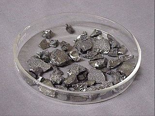
Boron is a chemical element; it has symbol B and atomic number 5. In its crystalline form it is a brittle, dark, lustrous metalloid; in its amorphous form it is a brown powder. As the lightest element of the boron group it has three valence electrons for forming covalent bonds, resulting in many compounds such as boric acid, the mineral sodium borate, and the ultra-hard crystals of boron carbide and boron nitride.

Chemical vapor deposition (CVD) is a vacuum deposition method used to produce high-quality, and high-performance, solid materials. The process is often used in the semiconductor industry to produce thin films.

MEMS is the technology of microscopic devices incorporating both electronic and moving parts. MEMS are made up of components between 1 and 100 micrometres in size, and MEMS devices generally range in size from 20 micrometres to a millimetre, although components arranged in arrays can be more than 1000 mm2. They usually consist of a central unit that processes data and several components that interact with the surroundings.
In materials science, a metal matrix composite (MMC) is a composite material with fibers or particles dispersed in a metallic matrix, such as copper, aluminum, or steel. The secondary phase is typically a ceramic or another metal. They are typically classified according to the type of reinforcement: short discontinuous fibers (whiskers), continuous fibers, or particulates. There is some overlap between MMCs and cermets, with the latter typically consisting of less than 20% metal by volume. When at least three materials are present, it is called a hybrid composite. MMCs can have much higher strength-to-weight ratios, stiffness, and ductility than traditional materials, so they are often used in demanding applications. MMCs typically have lower thermal and electrical conductivity and poor resistance to radiation, limiting their use in the very harshest environments.
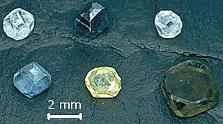
Lab-grown diamond is diamond that is produced in a controlled technological process. Unlike diamond simulants, synthetic diamonds are composed of the same material as naturally formed diamonds—pure carbon crystallized in an isotropic 3D form—and share identical chemical and physical properties.

Tungsten(VI) fluoride, also known as tungsten hexafluoride, is an inorganic compound with the formula WF6. It is a toxic, corrosive, colorless gas, with a density of about 13 kg/m3 (22 lb/cu yd). It is the only known gaseous transition metal compound and the densest known gas under standard ambient temperature and pressure. WF6 is commonly used by the semiconductor industry to form tungsten films, through the process of chemical vapor deposition. This layer is used in a low-resistivity metallic "interconnect". It is one of seventeen known binary hexafluorides.

Silicon nitride is a chemical compound of the elements silicon and nitrogen. Si
3N
4 is the most thermodynamically stable and commercially important of the silicon nitrides, and the term ″Silicon nitride″ commonly refers to this specific composition. It is a white, high-melting-point solid that is relatively chemically inert, being attacked by dilute HF and hot H
3PO
4. It is very hard. It has a high thermal stability with strong optical nonlinearities for all-optical applications.
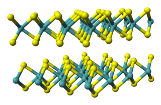
Tungsten disulfide is an inorganic chemical compound composed of tungsten and sulfur with the chemical formula WS2. This compound is part of the group of materials called the transition metal dichalcogenides. It occurs naturally as the rare mineral tungstenite. This material is a component of certain catalysts used for hydrodesulfurization and hydrodenitrification.
Electron-beam physical vapor deposition, or EBPVD, is a form of physical vapor deposition in which a target anode is bombarded with an electron beam given off by a charged tungsten filament under high vacuum. The electron beam causes atoms from the target to transform into the gaseous phase. These atoms then precipitate into solid form, coating everything in the vacuum chamber with a thin layer of the anode material.
Vacuum deposition is a group of processes used to deposit layers of material atom-by-atom or molecule-by-molecule on a solid surface. These processes operate at pressures well below atmospheric pressure. The deposited layers can range from a thickness of one atom up to millimeters, forming freestanding structures. Multiple layers of different materials can be used, for example to form optical coatings. The process can be qualified based on the vapor source; physical vapor deposition uses a liquid or solid source and chemical vapor deposition uses a chemical vapor.
Chemical vapour infiltration (CVI) is a ceramic engineering process whereby matrix material is infiltrated into fibrous preforms by the use of reactive gases at elevated temperature to form fiber-reinforced composites. The earliest use of CVI was the infiltration of fibrous alumina with chromium carbide. CVI can be applied to the production of carbon-carbon composites and ceramic-matrix composites. A similar technique is chemical vapour deposition (CVD), the main difference being that the deposition of CVD is on hot bulk surfaces, while CVI deposition is on porous substrates.

Hybrid physical–chemical vapor deposition (HPCVD) is a thin-film deposition technique, that combines physical vapor deposition (PVD) with chemical vapor deposition (CVD).

Zirconium diboride (ZrB2) is a highly covalent refractory ceramic material with a hexagonal crystal structure. ZrB2 is an ultra-high temperature ceramic (UHTC) with a melting point of 3246 °C. This along with its relatively low density of ~6.09 g/cm3 (measured density may be higher due to hafnium impurities) and good high temperature strength makes it a candidate for high temperature aerospace applications such as hypersonic flight or rocket propulsion systems. It is an unusual ceramic, having relatively high thermal and electrical conductivities, properties it shares with isostructural titanium diboride and hafnium diboride.

Solid is one of the four fundamental states of matter along with liquid, gas, and plasma. The molecules in a solid are closely packed together and contain the least amount of kinetic energy. A solid is characterized by structural rigidity and resistance to a force applied to the surface. Unlike a liquid, a solid object does not flow to take on the shape of its container, nor does it expand to fill the entire available volume like a gas. The atoms in a solid are bound to each other, either in a regular geometric lattice, or irregularly. Solids cannot be compressed with little pressure whereas gases can be compressed with little pressure because the molecules in a gas are loosely packed.

The vapor–liquid–solid method (VLS) is a mechanism for the growth of one-dimensional structures, such as nanowires, from chemical vapor deposition. The growth of a crystal through direct adsorption of a gas phase on to a solid surface is generally very slow. The VLS mechanism circumvents this by introducing a catalytic liquid alloy phase which can rapidly adsorb a vapor to supersaturation levels, and from which crystal growth can subsequently occur from nucleated seeds at the liquid–solid interface. The physical characteristics of nanowires grown in this manner depend, in a controllable way, upon the size and physical properties of the liquid alloy.
Ultra-high-temperature ceramics (UHTCs) are a type of refractory ceramics that can withstand extremely high temperatures without degrading, often above 2,000 °C. They also often have high thermal conductivities and are highly resistant to thermal shock, meaning they can withstand sudden and extreme changes in temperature without cracking or breaking. Chemically, they are usually borides, carbides, nitrides, and oxides of early transition metals.
Boron fiber or boron filament is an amorphous product which represents the major industrial use of elemental boron. Boron fiber manifests a combination of high strength and high elastic modulus.
Silicon carbide fibers are fibers ranging from 5 to 150 micrometres in diameter and composed primarily of silicon carbide molecules. Depending on manufacturing process, they may have some excess silicon or carbon, or have a small amount of oxygen. Relative to organic fibers and some ceramic fibers, silicon carbide fibers have high stiffness, high tensile strength, low weight, high chemical resistance, high temperature tolerance and low thermal expansion. (refs) These properties have made silicon carbide fiber the choice for hot section components in the next generation of gas turbines, e.g. the LEAP engine from GE.

Gilbert Daniel Nessim is a chemistry professor at Bar-Ilan University specializing in the synthesis of 1D and 2D nanomaterials for electronic, mechanic, and energy applications.
References
- ↑ Allen, S.D. (1981-11-01). "Laser chemical vapor deposition: A technique for selective area deposition". Journal of Applied Physics. 52 (11): 6501–6505. doi:10.1063/1.328600. ISSN 0021-8979.
- ↑ Method and Apparatus For the Freeform Growth of Three-Dimensional Structures Using Pressurized Precursor Flows and Growth Rate Control (US Patent # 5,786,023)
- ↑ Laser Assisted Fiber Growth (US Patent # 5,126,200)
- ↑ T. Wallenberger, Frederick & C. Nordine, Paul & Boman, Mats. (1994). “Inorganic fibers and microstructures directly from the vapor phase”. Composites Science and Technology v 51. pp. 193-212.
- ↑ T. Wallenberger, Frederick & C. Nordine, Paul. (1994). “Amorphous Silicon Nitride Fibers Grown from the Vapor Phase”. Journal of Materials Research v 9. pp. 527 - 530.
- ↑ Laser-assisted CVD Fabrication and Characterization of Carbon and Tungsten Microhelices for Microthrusters, Uppsala University, 2006, Dissertation, K.L. Williams
- ↑ Björklund, K.L & Lu, Jun & Heszler, P & Boman, Mats. (2002). “Kinetics, thermodynamics and microstructure of tungsten rods grown by thermal laser CVD”. Thin Solid Films v 416. pp. 41–48.
- ↑ Boman, Mats & Baeuerle, Dieter. (1995). “Laser‐Assisted Chemical Vapor Deposition of Boron”. Journal of the Chinese Chemical Society v 42.
- ↑ S. Harrison, J. Pegna, J. Schneiter, K.L. Williams, and R. Goduguchinta, (2017) “Laser Printed Ceramic Fiber Ribbons: Properties and Applications,” 2016 ICACC Proceedings/Ceramic Materials for Energy Applications VI, pp. 61-72
- ↑ Maxwell, James & Chavez, Craig & W. Springer, Robert & Maskaly, Karlene & Goodin, Dan. (2007). “Preparation of superhard BxCy fibers by microvortex-flow hyperbaric laser chemical vapor deposition”, Diamond and Related Materials v 16. pp. 1557-1564.
- ↑ Williams, K.L. & Jonsson, K & Köhler, Johan & Boman, Mats. (2007). “Electrothermal characterization of tungsten-coated carbon microcoils for micropropulsion systems”. Carbon v 45. pp. 484-492.
- ↑ Maxwell, James & Boman, Mats & W Springer, Robert & Narayan, Jaikumar & Gnanavelu, Saiprasanna. (2006). “Hyperbaric Laser Chemical Vapor Deposition of Carbon Fibers from the 1-Alkenes, 1-Alkynes, and Benzene”. Journal of the American Chemical Society v 128. pp. 4405-4413.
| | This industry-related article is a stub. You can help Wikipedia by expanding it. |