
Chemical vapor deposition (CVD) is a vacuum deposition method used to produce high quality, and high-performance, solid materials. The process is often used in the semiconductor industry to produce thin films.
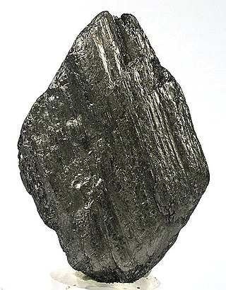
Graphite is a crystalline form of the element carbon. It consists of stacked layers of graphene. Graphite occurs naturally and is the most stable form of carbon under standard conditions. Synthetic and natural graphite are consumed on large scale for uses in pencils, lubricants, and electrodes. Under high pressures and temperatures it converts to diamond. It is a weak conductor of heat and electricity.
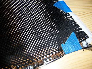
Carbon fibers or carbon fibres are fibers about 5 to 10 micrometers (0.00020–0.00039 in) in diameter and composed mostly of carbon atoms. Carbon fibers have several advantages: high stiffness, high tensile strength, high strength to weight ratio, high chemical resistance, high-temperature tolerance, and low thermal expansion. These properties have made carbon fiber very popular in aerospace, civil engineering, military, motorsports, and other competition sports. However, they are relatively expensive compared to similar fibers, such as glass fiber, basalt fibers, or plastic fibers.

The Czochralski method, also Czochralski technique or Czochralski process, is a method of crystal growth used to obtain single crystals of semiconductors, metals, salts and synthetic gemstones. The method is named after Polish scientist Jan Czochralski, who invented the method in 1915 while investigating the crystallization rates of metals. He made this discovery by accident: instead of dipping his pen into his inkwell, he dipped it in molten tin, and drew a tin filament, which later proved to be a single crystal.

Silicon carbide (SiC), also known as carborundum, is a hard chemical compound containing silicon and carbon. A semiconductor, it occurs in nature as the extremely rare mineral moissanite, but has been mass-produced as a powder and crystal since 1893 for use as an abrasive. Grains of silicon carbide can be bonded together by sintering to form very hard ceramics that are widely used in applications requiring high endurance, such as car brakes, car clutches and ceramic plates in bulletproof vests. Large single crystals of silicon carbide can be grown by the Lely method and they can be cut into gems known as synthetic moissanite.
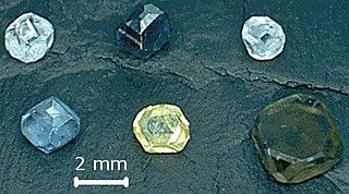
Lab-grown diamond is diamond that is produced in a controlled technological process. Unlike diamond simulants, synthetic diamonds are composed of the same material as naturally formed diamonds – pure carbon crystallized in an isotropic 3D form – and share identical chemical and physical properties.
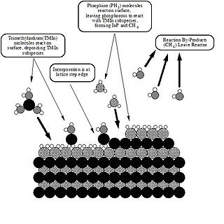
Metalorganic vapour-phase epitaxy (MOVPE), also known as organometallic vapour-phase epitaxy (OMVPE) or metalorganic chemical vapour deposition (MOCVD), is a chemical vapour deposition method used to produce single- or polycrystalline thin films. It is a process for growing crystalline layers to create complex semiconductor multilayer structures. In contrast to molecular-beam epitaxy (MBE), the growth of crystals is by chemical reaction and not physical deposition. This takes place not in vacuum, but from the gas phase at moderate pressures. As such, this technique is preferred for the formation of devices incorporating thermodynamically metastable alloys, and it has become a major process in the manufacture of optoelectronics, such as Light-emitting diodes. It was invented in 1968 at North American Aviation Science Center by Harold M. Manasevit.

Chromium(II) carbide is a ceramic compound that exists in several chemical compositions: Cr3C2, Cr7C3, and Cr23C6. At standard conditions it exists as a gray solid. It is extremely hard and corrosion resistant. It is also a refractory compound, which means that it retains its strength at high temperatures as well. These properties make it useful as an additive to metal alloys. When chromium carbide crystals are integrated into the surface of a metal it improves the wear resistance and corrosion resistance of the metal, and maintains these properties at elevated temperatures. The hardest and most commonly used composition for this purpose is Cr3C2.

Silicon nitride is a chemical compound of the elements silicon and nitrogen. Si
3N
4 is the most thermodynamically stable and commercially important of the silicon nitrides, and the term "silicon nitride" commonly refers to this specific composition. It is a white, high-melting-point solid that is relatively chemically inert, being attacked by dilute HF and hot H
3PO
4. It is very hard. It has a high thermal stability with strong optical nonlinearities for all-optical applications.
A micropipe, also called a micropore, microtube, capillary defect or pinhole defect, is a crystallographic defect in a single crystal substrate. Minimizing the presence of micropipes is important in semiconductor manufacturing, as their presence on a wafer can result in the failure of integrated circuits made from that wafer.
The micro-pulling-down (μ-PD) method is a crystal growth technique based on continuous transport of the melted substance through micro-channel(s) made in a crucible bottom. Continuous solidification of the melt is progressed on a liquid/solid interface positioned under the crucible. In a steady state, both the melt and the crystal are pulled-down with a constant velocity.
Carbide-derived carbon (CDC), also known as tunable nanoporous carbon, is the common term for carbon materials derived from carbide precursors, such as binary (e.g. SiC, TiC), or ternary carbides, also known as MAX phases (e.g., Ti2AlC, Ti3SiC2). CDCs have also been derived from polymer-derived ceramics such as Si-O-C or Ti-C, and carbonitrides, such as Si-N-C. CDCs can occur in various structures, ranging from amorphous to crystalline carbon, from sp2- to sp3-bonded, and from highly porous to fully dense. Among others, the following carbon structures have been derived from carbide precursors: micro- and mesoporous carbon, amorphous carbon, carbon nanotubes, onion-like carbon, nanocrystalline diamond, graphene, and graphite. Among carbon materials, microporous CDCs exhibit some of the highest reported specific surface areas (up to more than 3000 m2/g). By varying the type of the precursor and the CDC synthesis conditions, microporous and mesoporous structures with controllable average pore size and pore size distributions can be produced. Depending on the precursor and the synthesis conditions, the average pore size control can be applied at sub-Angstrom accuracy. This ability to precisely tune the size and shapes of pores makes CDCs attractive for selective sorption and storage of liquids and gases (e.g., hydrogen, methane, CO2) and the high electric conductivity and electrochemical stability allows these structures to be effectively implemented in electrical energy storage and capacitive water desalinization.
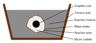
The Acheson process was invented by Edward Goodrich Acheson to synthesize silicon carbide (SiC) and graphite.
Roger Bacon was an American physicist and inventor at the Parma Technical Center of National Carbon Company in suburban Cleveland, Ohio, where he invented graphite fibers in 1958.

The sublimation sandwich method is a kind of physical vapor deposition used for creating man-made crystals. Silicon carbide is the most common crystal grown this way, though others crystals may also be created with it.
The Kyropoulos method, KY method, or Kyropoulos technique, is a method of bulk crystal growth used to obtain single crystals.
Shaping processes in crystal growth are a collection of techniques for growing bulk crystals of a defined shape from a melt, usually by constraining the shape of the liquid meniscus by means of a mechanical shaper. Crystals are commonly grown as fibers, solid cylinders, hollow cylinders, and sheets. More complex shapes such as tubes with a complex cross section, and domes have also been produced. Using a shaping process can produce a near net shape crystal and reduce the manufacturing cost for crystals which are composed of very expensive or difficult to machine materials.
Epitaxial graphene growth on silicon carbide (SiC) by thermal decomposition is a method to produce large-scale few-layer graphene (FLG). Graphene is one of the most promising nanomaterials for the future because of its various characteristics, like strong stiffness and high electric and thermal conductivity. Still, reproducible production of Graphene is difficult, thus many different techniques have been developed. The main advantage of epitaxial graphene growth on silicon carbide over other techniques is to obtain graphene layers directly on a semiconducting or semi-insulating substrate which is commercially available.

Low-energy plasma-enhanced chemical vapor deposition (LEPECVD) is a plasma-enhanced chemical vapor deposition technique used for the epitaxial deposition of thin semiconductor films. A remote low energy, high density DC argon plasma is employed to efficiently decompose the gas phase precursors while leaving the epitaxial layer undamaged, resulting in high quality epilayers and high deposition rates.
