A field-programmable gate array (FPGA) is a type of configurable integrated circuit that can be repeatedly programmed post manufacturing. FPGAs are a subset of logic devices referred to as programmable logic devices ("PLDs"). They consist of an array of programmable logic blocks with a connecting grid, that can be configured "in the field" to interconnect with other logic blocks to perform various digital functions. FPGAs are often used in limited (low) quantity production of custom-made products, and in research and development, where the higher cost of individual FPGAs is not as important, and where creating and manufacturing a custom circuit wouldn't be feasible. Other applications for FPGAs include the telecommunications, automotive, aerospace, and industrial sectors, which benefit from their flexibility, high signal processing speed, and parallel processing abilities.

An embedded system is a computer system—a combination of a computer processor, computer memory, and input/output peripheral devices—that has a dedicated function within a larger mechanical or electronic system. It is embedded as part of a complete device often including electrical or electronic hardware and mechanical parts. Because an embedded system typically controls physical operations of the machine that it is embedded within, it often has real-time computing constraints. Embedded systems control many devices in common use. In 2009, it was estimated that ninety-eight percent of all microprocessors manufactured were used in embedded systems.

AVR is a family of microcontrollers developed since 1996 by Atmel, acquired by Microchip Technology in 2016. These are modified Harvard architecture 8-bit RISC single-chip microcontrollers. AVR was one of the first microcontroller families to use on-chip flash memory for program storage, as opposed to one-time programmable ROM, EPROM, or EEPROM used by other microcontrollers at the time.
Reconfigurable computing is a computer architecture combining some of the flexibility of software with the high performance of hardware by processing with flexible hardware platforms like field-programmable gate arrays (FPGAs). The principal difference when compared to using ordinary microprocessors is the ability to add custom computational blocks using FPGAs. On the other hand, the main difference from custom hardware, i.e. application-specific integrated circuits (ASICs) is the possibility to adapt the hardware during runtime by "loading" a new circuit on the reconfigurable fabric, thus providing new computational blocks without the need to manufacture and add new chips to the existing system.
JTAG is an industry standard for verifying designs of and testing printed circuit boards after manufacture.

The NXP ColdFire is a microprocessor that derives from the Motorola 68000 family architecture, manufactured for embedded systems development by NXP Semiconductors. It was formerly manufactured by Freescale Semiconductor which merged with NXP in 2015.
Nucleus RTOS is a real-time operating system (RTOS) produced by the Embedded Software Division of Mentor Graphics, a Siemens Business, supporting 32- and 64-bit embedded system platforms. The operating system (OS) is designed for real-time embedded systems for medical, industrial, consumer, aerospace, and Internet of things (IoT) uses. Nucleus was released first in 1993. The latest version is 3.x, and includes features such as power management, process model, 64-bit support, safety certification, and support for heterogeneous computing multi-core system on a chip (SOCs) processors.

The Blackfin is a family of 16-/32-bit microprocessors developed, manufactured and marketed by Analog Devices. The processors have built-in, fixed-point digital signal processor (DSP) functionality performed by 16-bit multiply–accumulates (MACs), accompanied on-chip by a microcontroller. It was designed for a unified low-power processor architecture that can run operating systems while simultaneously handling complex numeric tasks such as real-time H.264 video encoding.
LEON is a radiation-tolerant 32-bit central processing unit (CPU) microprocessor core that implements the SPARC V8 instruction set architecture (ISA) developed by Sun Microsystems. It was originally designed by the European Space Research and Technology Centre (ESTEC), part of the European Space Agency (ESA), without any involvement by Sun. Later versions have been designed by Gaisler Research, under a variety of owners. It is described in synthesizable VHSIC Hardware Description Language (VHDL). LEON has a dual license model: An GNU Lesser General Public License (LGPL) and GNU General Public License (GPL) free and open-source software (FOSS) license that can be used without licensing fee, or a proprietary license that can be purchased for integration in a proprietary product. The core is configurable through VHDL generics, and is used in system on a chip (SOC) designs both in research and commercial settings.
The MicroBlaze is a soft microprocessor core designed for Xilinx field-programmable gate arrays (FPGA). As a soft-core processor, MicroBlaze is implemented entirely in the general-purpose memory and logic fabric of Xilinx FPGAs.
AVR32 is a 32-bit RISC microcontroller architecture produced by Atmel. The microcontroller architecture was designed by a handful of people educated at the Norwegian University of Science and Technology, including lead designer Øyvind Strøm and CPU architect Erik Renno in Atmel's Norwegian design center.

PSoC is a family of microcontroller integrated circuits by Cypress Semiconductor. These chips include a CPU core and mixed-signal arrays of configurable integrated analog and digital peripherals.
Intel Quartus Prime is programmable logic device design software produced by Intel; prior to Intel's acquisition of Altera the tool was called Altera Quartus Prime, earlier Altera Quartus II. Quartus Prime enables analysis and synthesis of HDL designs, which enables the developer to compile their designs, perform timing analysis, examine RTL diagrams, simulate a design's reaction to different stimuli, and configure the target device with the programmer. Quartus Prime includes an implementation of VHDL and Verilog for hardware description, visual editing of logic circuits, and vector waveform simulation.
Impulse C is a subset of the C programming language combined with a C-compatible function library supporting parallel programming, in particular for programming of applications targeting FPGA devices. It is developed by Impulse Accelerated Technologies of Kirkland, Washington.
LatticeMico32 is a 32-bit microprocessor reduced instruction set computer (RISC) soft core from Lattice Semiconductor optimized for field-programmable gate arrays (FPGAs). It uses a Harvard architecture, which means the instruction and data buses are separate. Bus arbitration logic can be used to combine the two buses, if desired.
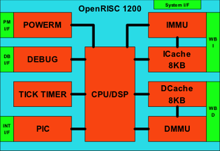
The OpenRISC 1200 (OR1200) is an implementation of the open source OpenRISC 1000 RISC architecture.
eSi-RISC is a configurable CPU architecture. It is available in five implementations: the eSi-1600, eSi-1650, eSi-3200, eSi-3250 and eSi-3264. The eSi-1600 and eSi-1650 feature a 16-bit data-path, while the eSi-32x0s feature 32-bit data-paths, and the eSi-3264 features a mixed 32/64-bit datapath. Each of these processors is licensed as soft IP cores, suitable for integrating into both ASICs and FPGAs.

The ARM Cortex-M is a group of 32-bit RISC ARM processor cores licensed by ARM Limited. These cores are optimized for low-cost and energy-efficient integrated circuits, which have been embedded in tens of billions of consumer devices. Though they are most often the main component of microcontroller chips, sometimes they are embedded inside other types of chips too. The Cortex-M family consists of Cortex-M0, Cortex-M0+, Cortex-M1, Cortex-M3, Cortex-M4, Cortex-M7, Cortex-M23, Cortex-M33, Cortex-M35P, Cortex-M52, Cortex-M55, Cortex-M85. A floating-point unit (FPU) option is available for Cortex-M4 / M7 / M33 / M35P / M52 / M55 / M85 cores, and when included in the silicon these cores are sometimes known as "Cortex-MxF", where 'x' is the core variant.

The ARM Cortex-R is a family of 32-bit and 64-bit RISC ARM processor cores licensed by Arm Ltd. The cores are optimized for hard real-time and safety-critical applications. Cores in this family implement the ARM Real-time (R) profile, which is one of three architecture profiles, the other two being the Application (A) profile implemented by the Cortex-A family and the Microcontroller (M) profile implemented by the Cortex-M family. The ARM Cortex-R family of microprocessors currently consists of ARM Cortex-R4(F), ARM Cortex-R5(F), ARM Cortex-R7(F), ARM Cortex-R8(F), ARM Cortex-R52(F), ARM Cortex-R52+(F), and ARM Cortex-R82(F).
OVPsim is a multiprocessor platform emulator used to run unchanged production binaries of the target hardware. It has public APIs allowing users to create their own processor, peripheral and platform models. Various models are available as open source. OVPsim is a key component of the Open Virtual Platforms initiative (OVP), an organization created to promote the use of open virtual platforms for embedded software development. OVPsim requires OVP registration to download.