Logic block

Last updated

In computing, a logic block or configurable logic block (CLB) is a fundamental building block of field-programmable gate array (FPGA) technology.[ citation needed ] Logic blocks can be configured by the engineer to provide reconfigurable logic gates.[ citation needed ]

Contents

Logic blocks are the most common FPGA architecture, and are usually laid out within a logic block array.[ citation needed ] Logic blocks require I/O pads (to interface with external signals), and routing channels (to interconnect logic blocks).

Programmable logic blocks were invented by David W. Page and LuVerne R. Peterson, and defined within their 1985 patents. [1] [2]

Applications

An application circuit must be mapped into an FPGA with adequate resources. While the number of logic blocks and I/Os required is easily determined from the design, the number of routing tracks needed may vary considerably even among designs with the same amount of logic.

For example, a crossbar switch requires much more routing than a systolic array with the same gate count. Since unused routing tracks increase the cost (and decrease the performance) of the part without providing any benefit, FPGA manufacturers try to provide just enough tracks so that most designs that will fit in terms of lookup tables (LUTs) and I/Os can be routed. This is determined by estimates such as those derived from Rent's rule or by experiments with existing designs.

FPGAs are also widely used for systems validation including pre-silicon validation, post-silicon validation, and firmware development. This allows chip companies to validate their design before the chip is produced in the factory, reducing the time-to-market.

Architecture

Simplified illustration of a logic cell FPGA cell example.png
Simplified illustration of a logic cell

In general, a logic block consists of a few logic cells (each cell is called an adaptive logic module (ALM), a logic element (LE), slice, etc.). A typical cell consists of a 4-input LUT, a full adder (FA), and a D-type flip-flop (DFF), as shown to the right. The LUTs are in this figure split into two 3-input LUTs. In normal mode those are combined into a 4-input LUT through the left mux. In arithmetic mode, their outputs are fed to the FA. The selection of mode is programmed into the middle multiplexer. The output can be either synchronous or asynchronous, depending on the programming of the mux to the right, in the figure example. In practice, entire or parts of the FA are put as functions into the LUTs in order to save space. [3] [4] [5]

Logic blocks typically contain a few ALMs/LEs/slices. ALMs and slices usually contain 2 or 4 structures similar to the example figure, with some shared signals.

Manufacturers have started moving to 6-input LUTs in their high performance parts, claiming increased performance. [6]

3D architecture

To shrink the size and power consumption of FPGAs, vendors such as Tabula and Xilinx have introduced new 3D or stacked architectures. [7] [8] Following the introduction of its 28 nm 7-series FPGAs, Xilinx revealed that several of the highest-density parts in those FPGA product lines will be constructed using multiple dies in one package, employing technology developed for 3D construction and stacked-die assemblies. The technology stacks several (three or four) active FPGA dice side-by-side on a silicon interposer  – a single piece of silicon that carries passive interconnect. [8] [9] The multi-die construction also allows different parts of the FPGA to be created with different process technologies, as the process requirements are different between the FPGA fabric itself and the very high speed 28 Gbit/s serial transceivers. An FPGA built in this way is called a heterogeneous FPGA. [10]

External I/O

Logic block pin locations Logic block pins.svg
Logic block pin locations

Since clock signals (and often other high-fan-out signals) are normally routed via special-purpose dedicated routing networks (i.e. global buffers) in commercial FPGAs, they and other signals are separately managed.

For this example architecture, the locations of the FPGA logic block pins are shown to the right.

Each input is accessible from one side of the logic block, while the output pin can connect to routing wires in both the channel to the right and the channel below the logic block.

Each logic block output pin can connect to any of the wiring segments in the channels adjacent to it.

Similarly, an I/O pad can connect to any one of the wiring segments in the channel adjacent to it. For example, an I/O pad at the top of the chip can connect to any of the W wires (where W is the channel width) in the horizontal channel immediately below it.

Routing

Generally, the FPGA routing is unsegmented. That is, each wiring segment spans only one logic block before it terminates in a switch box. By turning on some of the programmable switches within a switch box, longer paths can be constructed. For higher speed interconnect, some FPGA architectures use longer routing lines that span multiple logic blocks.

Switch box topology Switch box.svg
Switch box topology

Whenever a vertical and a horizontal channel intersect, there is a switch box. In this architecture, when a wire enters a switch box, there are three programmable switches that allow it to connect to three other wires in adjacent channel segments. The pattern, or topology, of switches used in this architecture is the planar or domain-based switch box topology. In this switch box topology, a wire in track number one connects only to wires in track number one in adjacent channel segments, wires in track number 2 connect only to other wires in track number 2 and so on. The figure on the right illustrates the connections in a switch box.

Generally, all the routing channels have the same width (number of wires). Multiple I/O pads may fit into the height of one row or the width of one column in the array.

Hard blocks

Modern FPGA families expand upon the above capabilities to include higher level functionality fixed into the silicon. Having these common functions embedded into the silicon reduces the area required and gives those functions increased speed compared to building them from primitives. Examples of these include multipliers, generic DSP blocks, embedded processors, high speed I/O logic and embedded memories.

Higher-end FPGAs can contain high speed multi-gigabit transceivers and hard IP cores such as processor cores, Ethernet media access controllers, PCI/PCI Express controllers, and external memory controllers. These cores exist alongside the programmable fabric, but they are built out of transistors instead of LUTs so they have ASIC level performance and power consumption while not consuming a significant amount of fabric resources, leaving more of the fabric free for the application-specific logic. The multi-gigabit transceivers also contain high performance analog input and output circuitry along with high-speed serializers and deserializers, components which cannot be built out of LUTs. Higher-level PHY layer functionality such as line coding may or may not be implemented alongside the serializers and deserializers in hard logic, depending on the FPGA.

Clock signals

Most of the circuitry built inside of an FPGA is synchronous circuitry that requires a clock signal. FPGAs contain dedicated global and regional routing networks for clock and reset so they can be delivered with minimal skew. FPGAs generally contain analog phase-locked loop and/or delay-locked loop components to synthesize new clock frequencies and attenuate jitter. Complex designs can use multiple clocks with different frequency and phase relationships, each forming separate clock domains. These clock signals can be generated locally by an oscillator or they can be recovered from a high speed serial data stream. Care must be taken when building clock domain crossing circuitry to avoid metastability. FPGAs generally contain block RAMs that are capable of working as dual port RAMs with different clocks, aiding in the construction of building FIFOs and dual port buffers that connect differing clock domains.

See also

Related Research Articles

Processor design is a subfield of computer science and computer engineering (fabrication) that deals with creating a processor, a key component of computer hardware.

<span class="mw-page-title-main">Field-programmable gate array</span> Array of logic gates that are reprogrammable

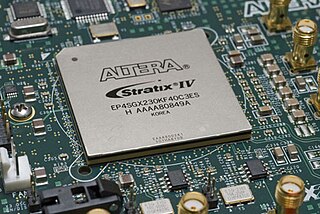
A field-programmable gate array (FPGA) is a type of configurable integrated circuit that can be programmed or reprogrammed after manufacturing. FPGAs are part of a broader set of logic devices referred to as programmable logic devices (PLDs). They consist of an array of programmable logic blocks and interconnects that can be configured to perform various digital functions. FPGAs are commonly used in applications where flexibility, speed, and parallel processing capabilities are required, such as in telecommunications, automotive, aerospace, and industrial sectors.

<span class="mw-page-title-main">Programmable logic device</span> Reconfigurable digital circuit element

A programmable logic device (PLD) is an electronic component used to build reconfigurable digital circuits. Unlike digital logic constructed using discrete logic gates with fixed functions, the function of a PLD is undefined at the time of manufacture. Before the PLD can be used in a circuit it must be programmed to implement the desired function. Compared to fixed logic devices, programmable logic devices simplify the design of complex logic and may offer superior performance. Unlike for microprocessors, programming a PLD changes the connections made between the gates in the device.

<span class="mw-page-title-main">Front-side bus</span> Type of computer communication interface

The front-side bus (FSB) is a computer communication interface (bus) that was often used in Intel-chip-based computers during the 1990s and 2000s. The EV6 bus served the same function for competing AMD CPUs. Both typically carry data between the central processing unit (CPU) and a memory controller hub, known as the northbridge.

Reconfigurable computing is a computer architecture combining some of the flexibility of software with the high performance of hardware by processing with flexible hardware platforms like field-programmable gate arrays (FPGAs). The principal difference when compared to using ordinary microprocessors is the ability to add custom computational blocks using FPGAs. On the other hand, the main difference from custom hardware, i.e. application-specific integrated circuits (ASICs) is the possibility to adapt the hardware during runtime by "loading" a new circuit on the reconfigurable fabric, thus providing new computational blocks without the need to manufacture and add new chips to the existing system.

JTAG is an industry standard for verifying designs of and testing printed circuit boards after manufacture.

<span class="mw-page-title-main">Xilinx</span> American technology company

Xilinx, Inc. was an American technology and semiconductor company that primarily supplied programmable logic devices. The company is known for inventing the first commercially viable field-programmable gate array (FPGA). It also created the first fabless manufacturing model.

In digital circuit design, register-transfer level (RTL) is a design abstraction which models a synchronous digital circuit in terms of the flow of digital signals (data) between hardware registers, and the logical operations performed on those signals.

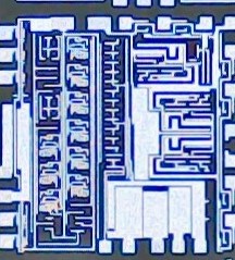
Place and route is a stage in the design of printed circuit boards, integrated circuits, and field-programmable gate arrays. As implied by the name, it is composed of two steps, placement and routing. The first step, placement, involves deciding where to place all electronic components, circuitry, and logic elements in a generally limited amount of space. This is followed by routing, which decides the exact design of all the wires needed to connect the placed components. This step must implement all the desired connections while following the rules and limitations of the manufacturing process.

<span class="mw-page-title-main">Complex programmable logic device</span> Type of electronic component

A complex programmable logic device (CPLD) is a programmable logic device with complexity between that of PALs and FPGAs, and architectural features of both. The main building block of the CPLD is a macrocell, which contains logic implementing disjunctive normal form expressions and more specialized logic operations.

<span class="mw-page-title-main">Mixed-signal integrated circuit</span> Integrated circuit

A mixed-signal integrated circuit is any integrated circuit that has both analog circuits and digital circuits on a single semiconductor die. Their usage has grown dramatically with the increased use of cell phones, telecommunications, portable electronics, and automobiles with electronics and digital sensors.

Asynchronous circuit is a sequential digital logic circuit that does not use a global clock circuit or signal generator to synchronize its components. Instead, the components are driven by a handshaking circuit which indicates a completion of a set of instructions. Handshaking works by simple data transfer protocols. Many synchronous circuits were developed in early 1950s as part of bigger asynchronous systems. Asynchronous circuits and theory surrounding is a part of several steps in integrated circuit design, a field of digital electronics engineering.

A multi-gigabit transceiver (MGT) is a SerDes capable of operating at serial bit rates above 1 Gigabit/second. MGTs are used increasingly for data communications because they can run over longer distances, use fewer wires, and thus have lower costs than parallel interfaces with equivalent data throughput.

QPACE is a massively parallel and scalable supercomputer designed for applications in lattice quantum chromodynamics.

Field-programmable gate array prototyping, also referred to as FPGA-based prototyping, ASIC prototyping or system-on-chip (SoC) prototyping, is the method to prototype system-on-chip and application-specific integrated circuit designs on FPGAs for hardware verification and early software development.

Computing with Memory refers to computing platforms where function response is stored in memory array, either one or two-dimensional, in the form of lookup tables (LUTs) and functions are evaluated by retrieving the values from the LUTs. These computing platforms can follow either a purely spatial computing model, as in field-programmable gate array (FPGA), or a temporal computing model, where a function is evaluated across multiple clock cycles. The latter approach aims at reducing the overhead of programmable interconnect in FPGA by folding interconnect resources inside a computing element. It uses dense two-dimensional memory arrays to store large multiple-input multiple-output LUTs. Computing with Memory differs from Computing in Memory or processor-in-memory (PIM) concepts, widely investigated in the context of integrating a processor and memory on the same chip to reduce memory latency and increase bandwidth. These architectures seek to reduce the distance the data travels between the processor and the memory. The Berkeley IRAM project is one notable contribution in the area of PIM architectures.

Virtex is the flagship family of FPGA products currently developed by AMD, originally Xilinx before being acquired by the former. Other current product lines include Kintex (mid-range) and Artix (low-cost), each including configurations and models optimized for different applications. In addition, AMD offers the Spartan low-cost series, which continues to be updated and is nearing production utilizing the same underlying architecture and process node as the larger 7-series devices.

<span class="mw-page-title-main">Tabula, Inc.</span>

Tabula, Inc., was an American fabless semiconductor company based in Santa Clara, California. Founded in 2003 by Steve Teig, it raised $215 million in venture funding. The company designed and built three dimensional field programmable gate arrays and ranked third on the Wall Street Journal's annual "Next Big Thing" list in 2012.

A field-programmable object array (FPOA) is a class of programmable logic devices designed to be modified or programmed after manufacturing. They are designed to bridge the gap between ASIC and FPGA. They contain a grid of programmable silicon objects. Arrix range of FPOA contained three types of silicon objects: arithmetic logic units (ALUs), register files (RFs) and multiply-and-accumulate units (MACs). Both the objects and interconnects are programmable.

Verilog-to-Routing (VTR) is an open source CAD flow for FPGA devices. VTR's main purpose is to map a given circuit described in Verilog, a Hardware Description Language, on a given FPGA architecture for research and development purposes; the FPGA architecture targeted could be a novel architecture that a researcher wishes to explore, or it could be an existing commercial FPGA whose architecture has been captured in the VTR input format. The VTR project has many contributors, with lead collaborating universities being the University of Toronto, the University of New Brunswick, and the University of California, Berkeley. Additional contributors include Google, The University of Utah, Princeton University, Altera, Intel, Texas Instruments, and MIT Lincoln Lab.

References

  1. Google Patent Search, "Re-programmable PLA". Filed January 11, 1983. Granted April 2, 1985. Retrieved February 5, 2009.
  2. Google Patent Search, "Dynamic data re-programmable PLA". Filed January 11, 1983. Granted June 18, 1985. Retrieved February 5, 2009.
  3. "Cyclone II Device Handbook, Volume 1 : Cyclone II Architecture - functional description" (PDF). Altera . 2007.
  4. "Documentation: Stratix IV Devices" (PDF). Altera.com. 2008-06-11. Archived from the original (PDF) on 2011-09-26. Retrieved 2013-05-01.
  5. http://www.xilinx.com/support/documentation/user_guides/ug070.pdf [ bare URL PDF ]
  6. http://www.origin.xilinx.com/support/documentation/white_papers/wp245.pdf [ bare URL PDF ]
  7. Dean Takahashi, VentureBeat. "Intel connection helped chip startup Tabula raise $108M." May 2, 2011. Retrieved May 13, 2011.
  8. 1 2 Lawrence Latif, The Inquirer. "FPGA manufacturer claims to beat Moore's Law." October 27, 2010. Retrieved May 12, 2011.
  9. EDN Europe. "Xilinx adopts stacked-die 3D packaging." November 1, 2010. Retrieved May 12, 2011.
  10. http://www.xilinx.com/support/documentation/white_papers/wp380_Stacked_Silicon_Interconnect_Technology.pdf [ bare URL PDF ]