This article's lead sectionmay be too short to adequately summarize the key points. Please consider expanding the lead to provide an accessible overview of all important aspects of the article.(November 2014)
PCI configuration space is the underlying way that the Conventional PCI, PCI-X and PCI Express perform auto configuration of the cards inserted into their bus.
PCI devices have a set of registers referred to as configuration space and PCI Express introduces extended configuration space for devices. Configuration space registers are mapped to memory locations. Device drivers and diagnostic software must have access to the configuration space, and operating systems typically use APIs to allow access to device configuration space. When the operating system does not have access methods defined or APIs for memory mapped configuration space requests, the driver or diagnostic software has the burden to access the configuration space in a manner that is compatible with the operating system's underlying access rules. In all systems, device drivers are encouraged to use APIs provided by the operating system to access the configuration space of the device.
One of the major improvements the PCI Local Bus had over other I/O architectures was its configuration mechanism. In addition to the normal memory-mapped and I/O port spaces, each device function on the bus has a configuration space, which is 256 bytes long, addressable by knowing the eight-bit PCI bus, five-bit device, and three-bit function numbers for the device (commonly referred to as the BDF or B/D/F, as abbreviated from bus/device/function). This allows up to 256 buses, each with up to 32 devices, each supporting eight functions. A single PCI expansion card can respond as a device and must implement at least function number zero. The first 64 bytes of configuration space are standardized; the remainder are available for vendor-defined purposes. Some high-end computers support more than one PCI domain (or PCI segment); each PCI domain supports up to 256 buses.
In order to allow more parts of configuration space to be standardized without conflicting with existing uses, there can be a list of capabilities defined within the remaining 192 bytes of PCI configuration space. Each capability has one byte that describes which capability it is, and one byte to point to the next capability. The number of additional bytes depends on the capability ID. If capabilities are being used, a bit in the Status register is set, and a pointer to the first in a linked list of capabilities is provided in the Cap. pointer register defined in the Standardized Registers.
PCI-X 2.0 and PCI Express introduced an extended configuration space, up to 4096 bytes. The only standardized part of extended configuration space is the first four bytes at 0x100 which are the start of an extended capability list. Extended capabilities are very much like normal capabilities except that they can refer to any byte in the extended configuration space (by using 12 bits instead of eight), have a four-bit version number and a 16-bit capability ID. Extended capability IDs overlap with normal capability IDs, but there is no chance of confusion as they are in separate lists.
Standardized registers
Standard registers of PCI Type 0 (Non-Bridge) Configuration Space Header
The Device ID (DID) and Vendor ID (VID) registers identify the device (such as an IC), and are commonly called the PCI ID. The 16-bit vendor ID is allocated by the PCI-SIG. The 16-bit device ID is then assigned by the vendor. There is an inactive project to collect all known Vendor and Device IDs. (See the external links below.)
The Status register is used to report which features are supported and whether certain kinds of errors have occurred. The Command register contains a bitmask of features that can be individually enabled and disabled. The Header Type register values determine the different layouts of remaining 48 bytes (64-16) of the header, depending on the function of the device. That is, Type 1 headers for Root Complex, switches, and bridges. Then Type 0 for endpoints. The Cache Line Size register must be programmed before the device is told it can use the memory-write-and-invalidate transaction. This should normally match the CPU's cache line size, but the correct setting is system dependent. This register does not apply to PCI Express.
The Subsystem ID (SSID) and the Subsystem Vendor ID (SVID) differentiate specific model (such as an add-in card). While the Vendor ID is that of the chipset manufacturer, the Subsystem Vendor ID is that of the card manufacturer. The Subsystem ID is assigned by the subsystem vendor from the same number space as the Device ID. As an example, in the case of wireless network cards, the chip manufacturer might be Broadcom or Atheros, and the card manufacturer might be Netgear or Hewlett-Packard. Generally, the Vendor ID–Device ID combination designates which driver the host should load in order to handle the device, as all cards with the same VID:DID combination can be handled by the same driver. The Subsystem Vendor ID–Subsystem ID combination identifies the card, which is the kind of information the driver may use to apply a minor card-specific change in its operation.
Bus enumeration
To address a PCI device, it must be enabled by being mapped into the system's I/O port address space or memory-mapped address space. The system's firmware (e.g. BIOS) or the operating system program the Base Address Registers (commonly called BARs) to inform the device of its resources configuration by writing configuration commands to the PCI controller. Because all PCI devices are in an inactive state upon system reset, they will have no addresses assigned to them by which the operating system or device drivers can communicate with them. Either the BIOS or the operating system geographically addresses the PCI devices (for example, the first PCI slot, the second PCI slot, the third PCI slot, or the integrated PCI devices, etc., on the motherboard) through the PCI controller using the per slot or per device IDSEL (Initialization Device Select) signals.
When the computer is powered on, the PCI bus(es) and device(s) must be enumerated by BIOS or operating system. Bus enumeration is performed by attempting to access the PCI configuration space registers for each buses, devices and functions. Note that device number, different from VID and DID, is merely a device's sequential number on that bus. Moreover, after a new bridge is detected, a new bus number is defined, and device enumeration restarts at device number zero.
If no response is received from the device's function #0, the bus master performs an abort and returns an all-bits-on value (FFFFFFFF in hexadecimal), which is an invalid VID/DID value, thus the BIOS or operating system can tell that the specified combination bus/device_number/function (B/D/F) is not present. So, when a read to a function ID of zero for a given bus/device causes the master (initiator) to abort, it must then be presumed that no working device exists on that bus because devices are required to implement function number zero. In this case, reads to the remaining functions numbers (1–7) are not necessary as they also will not exist.
When a read to a specified B/D/F combination for the vendor ID register succeeds, the system firmware or operating system knows that it exists; it writes all ones to its BARs and reads back the device's requested memory size in an encoded form. The design implies that all address space sizes are a power of two and are naturally aligned.[1]
At this point, the BIOS or operating system will program the memory-mapped addresses and I/O port addresses into the device's BAR configuration registers. These addresses stay valid as long as the system remains turned on. Upon power-off, these settings are lost and the procedure is repeated next time the system is powered back on. The BIOS or operating system will also program some other registers of the PCI configuration space for each PCI device, e.g. interrupt request. Since this entire process is fully automated, the user is spared the task of configuring any newly added hardware manually by changing DIP switches on the cards themselves. This automatic device discovery and address space assignment is how plug and play is implemented.
If a PCI-to-PCI bridge is found, the system must assign the secondary PCI bus beyond the bridge a bus number other than zero, and then enumerate the devices on that secondary bus. If more PCI bridges are found, the discovery continues recursively until all possible domain/bus/device combinations are scanned.
Each non-bridge PCI device function can implement up to 6 BARs, each of which can respond to different addresses in I/O port and memory-mapped address space. Each BAR describes a region [2][1] that is between 16 bytes and 2 gigabytes in size, located below the 4 gigabyte address space limit. If a platform supports the "Above 4G" option in system firmware, 64 bit BARs can be used. Resizable BAR (also known as Re-Size BAR, AMDSmart Access Memory (SAM),[3] or ASRockClever Access Memory (CAM))[4] is a capability which a PCIe device can use to negotiate a larger BAR size.[5] Classically, BARs were limited to a size of 256MB, but modern graphics cards have framebuffers much larger than that.[3] This mismatch led to inefficiencies when the CPU accessed the framebuffer.[3] Resizable BAR lets a CPU access the whole framebuffer at once, thus improving performance.[3]
When performing a Configuration Space access, a PCI device does not decode the address to determine if it should respond, but instead looks at the Initialization Device Select signal (IDSEL). There is a system-wide unique activation method for each IDSEL signal. The PCI device is required to decode only the lowest order 11 bits of the address space (AD[10] to AD[0]) address/data signals, and can ignore decoding the 21 high order A/D signals (AD[31] to AD[11]) because a Configuration Space access implementation has each slot's IDSEL pin connected to a different high order address/data line AD[11] through AD[31]. The IDSEL signal is a different pin for each PCI device/adapter/slot.
To configure the card in slot n, the PCI bus bridge performs a configuration-space access cycle with the PCI device's register to be addressed on lines AD[7:2] (AD[1:0] are always zero since registers are double words (32-bits)), and the PCI function number specified on bits AD[10:8], with all higher-order bits zeros except for AD[n+11] being used as the IDSEL signal on a given slot/device.
To reduce electrically loading down the timing critical (and thus electrically loading sensitive) AD[] bus, the IDSEL signal on the PCI slot connector is usually connected to its assigned AD[n+11] pin through a resistor. This causes the PCI's IDSEL signal to reach its active condition more slowly than other PCI bus signals (due to the RC time constant of both the resistor and the IDSEL pin's input capacitance). Thus Configuration Space accesses are performed more slowly to allow time for the IDSEL signal to reach a valid level.
The scanning on the bus is performed on the Intel platform by accessing two defined standardized ports. These ports are the Configuration Space Address (0xCF8) I/O port and Configuration Space Data (0xCFC) I/O port. The value written to the Configuration Space Address I/O port is created by combining B/D/F values and the registers address value into a 32-bit word.
Software implementation
Configuration reads and writes can be initiated from the CPU in two ways: one legacy method via I/O addresses 0xCF8 and 0xCFC, and another called memory-mapped configuration.[6]
The legacy method was present in the original PCI, and it is called Configuration Access Mechanism (CAM). It allows for 256 bytes of a device's address space to be reached indirectly via two 32-bit registers called PCI CONFIG_ADDRESS and PCI CONFIG_DATA. These registers are at addresses 0xCF8 and 0xCFC in the x86 I/O address space.[7] For example, a software driver (firmware, OS kernel or kernel driver) can use these registers to configure a PCI device by writing the address of the device's register into CONFIG_ADDRESS, and by putting the data that is supposed to be written to the device into CONFIG_DATA. Since this process requires a write to a register in order to write the device's register, it is referred to as "indirection".
The format of CONFIG_ADDRESS is the following:
0x80000000|bus<<16|device<<11|function<<8|offset
As explained previously, addressing a device via Bus, Device, and Function (BDF) is also referred to as "addressing a device geographically." See arch/x86/pci/early.c in the Linux kernel code for an example of code that uses geographical addressing.[8]
When extended configuration space is used on some AMD CPUs, the extra bits 11:8 of the offset are written to bits 27:24 of the CONFIG_ADDRESS register:[9][10]
The second method was created for PCI Express. It is called Enhanced Configuration Access Mechanism (ECAM). It extends device's configuration space to 4KB, with the bottom 256 bytes overlapping the original (legacy) configuration space in PCI. The section of the addressable space is "stolen" so that the accesses from the CPU don't go to memory but rather reach a given device in the PCI Express fabric. During system initialization, BIOS determines the base address for this "stolen" address region and communicates it to the root complex and to the operating system.
Each device has its own 4KB space and each device's info is accessible through a simple array dev[bus][device][function] so that 256MB of physical contiguous space is "stolen" for this use (256 buses × 32 devices × 8 functions × 4KB = 256MB). The base physical address of this array is not specified. For example, on modern x86 systems the ACPI tables contain the necessary information.[11]
Accelerated Graphics Port (AGP) is a parallel expansion card standard, designed for attaching a video card to a computer system to assist in the acceleration of 3D computer graphics. It was originally designed as a successor to PCI-type connections for video cards. Since 2004, AGP was progressively phased out in favor of PCI Express (PCIe), which is serial, as opposed to parallel; by mid-2008, PCI Express cards dominated the market and only a few AGP models were available, with GPU manufacturers and add-in board partners eventually dropping support for the interface in favor of PCI Express.
Industry Standard Architecture (ISA) is the 16-bit internal bus of IBM PC/AT and similar computers based on the Intel 80286 and its immediate successors during the 1980s. The bus was (largely) backward compatible with the 8-bit bus of the 8088-based IBM PC, including the IBM PC/XT as well as IBM PC compatibles.
Peripheral Component Interconnect (PCI) is a local computer bus for attaching hardware devices in a computer and is part of the PCI Local Bus standard. The PCI bus supports the functions found on a processor bus but in a standardized format that is independent of any given processor's native bus. Devices connected to the PCI bus appear to a bus master to be connected directly to its own bus and are assigned addresses in the processor's address space. It is a parallel bus, synchronous to a single bus clock. Attached devices can take either the form of an integrated circuit fitted onto the motherboard or an expansion card that fits into a slot. The PCI Local Bus was first implemented in IBM PC compatibles, where it displaced the combination of several slow Industry Standard Architecture (ISA) slots and one fast VESA Local Bus (VLB) slot as the bus configuration. It has subsequently been adopted for other computer types. Typical PCI cards used in PCs include: network cards, sound cards, modems, extra ports such as Universal Serial Bus (USB) or serial, TV tuner cards and hard disk drive host adapters. PCI video cards replaced ISA and VLB cards until rising bandwidth needs outgrew the abilities of PCI. The preferred interface for video cards then became Accelerated Graphics Port (AGP), a superset of PCI, before giving way to PCI Express.
Direct memory access (DMA) is a feature of computer systems that allows certain hardware subsystems to access main system memory independently of the central processing unit (CPU).
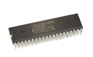
The Intel MCS-51 is a single chip microcontroller (MCU) series developed by Intel in 1980 for use in embedded systems. The architect of the Intel MCS-51 instruction set was John H. Wharton. Intel's original versions were popular in the 1980s and early 1990s, and enhanced binary compatible derivatives remain popular today. It is a complex instruction set computer, but also has some of the features of RISC architectures, such as a large register set and register windows, and has separate memory spaces for program instructions and data.
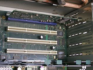
In computing, an expansion card is a printed circuit board that can be inserted into an electrical connector, or expansion slot on a computer's motherboard to add functionality to a computer system. Sometimes the design of the computer's case and motherboard involves placing most of these slots onto a separate, removable card. Typically such cards are referred to as a riser card in part because they project upward from the board and allow expansion cards to be placed above and parallel to the motherboard.
Real mode, also called real address mode, is an operating mode of all x86-compatible CPUs. The mode gets its name from the fact that addresses in real mode always correspond to real locations in memory. Real mode is characterized by a 20-bit segmented memory address space and unlimited direct software access to all addressable memory, I/O addresses and peripheral hardware. Real mode provides no support for memory protection, multitasking, or code privilege levels.
I2C (Inter-Integrated Circuit; pronounced as “eye-squared-see” or “eye-two-see”), alternatively known as I2C or IIC, is a synchronous, multi-master/multi-slave (controller/target), single-ended, serial communication bus invented in 1982 by Philips Semiconductors. It is widely used for attaching lower-speed peripheral ICs to processors and microcontrollers in short-distance, intra-board communication.
In computer architecture, 64-bit integers, memory addresses, or other data units are those that are 64 bits wide. Also, 64-bit central processing units (CPU) and arithmetic logic units (ALU) are those that are based on processor registers, address buses, or data buses of that size. A computer that uses such a processor is a 64-bit computer.
x86 assembly language is the name for the family of assembly languages which provide some level of backward compatibility with CPUs back to the Intel 8008 microprocessor, which was launched in April 1972. It is used to produce object code for the x86 class of processors.
Memory-mapped I/O (MMIO) and port-mapped I/O (PMIO) are two complementary methods of performing input/output (I/O) between the central processing unit (CPU) and peripheral devices in a computer. An alternative approach is using dedicated I/O processors, commonly known as channels on mainframe computers, which execute their own instructions.
In IBM PC compatible computing, DOS memory management refers to software and techniques employed to give applications access to more than 640 kibibytes (KiB) of "conventional memory". The 640 KiB limit was specific to the IBM PC and close compatibles; other machines running MS-DOS had different limits, for example the Apricot PC could have up to 768 KiB and the Sirius Victor 9000, 896 KiB. Memory management on the IBM family was made complex by the need to maintain backward compatibility to the original PC design and real-mode DOS, while allowing computer users to take advantage of large amounts of low-cost memory and new generations of processors. Since DOS has given way to Microsoft Windows and other 32-bit operating systems not restricted by the original arbitrary 640 KiB limit of the IBM PC, managing the memory of a personal computer no longer requires the user to manually manipulate internal settings and parameters of the system.
In computing, Physical Address Extension (PAE), sometimes referred to as Page Address Extension, is a memory management feature for the x86 architecture. PAE was first introduced by Intel in the Pentium Pro, and later by AMD in the Athlon processor. It defines a page table hierarchy of three levels (instead of two), with table entries of 64 bits each instead of 32, allowing these CPUs to directly access a physical address space larger than 4 gigabytes (232 bytes).
Autoconfig is an auto-configuration protocol of Amiga computers which is intended to automatically assign resources to expansion devices without the need for jumper settings. It is analogous to PCI configuration through ACPI.
PCI-X, short for Peripheral Component Interconnect eXtended, is a computer bus and expansion card standard that enhances the 32-bit PCI local bus for higher bandwidth demanded mostly by servers and workstations. It uses a modified protocol to support higher clock speeds, but is otherwise similar in electrical implementation. PCI-X 2.0 added speeds up to 533 MHz, with a reduction in electrical signal levels.
An Option ROM for the PC platform is a piece of firmware that resides in ROM on an expansion card, which gets executed to initialize the device and (optionally) add support for the device to the BIOS. In its usual use, it is essentially a driver that interfaces between the BIOS API and hardware. Technically, an option ROM is firmware that is executed by the BIOS after POST and before the BIOS boot process, gaining complete control of the system and being generally unrestricted in what it can do. The BIOS relies on each option ROM to return control to the BIOS so that it can either call the next option ROM or commence the boot process. For this reason, it is possible for an option ROM to keep control and preempt the BIOS boot process. The BIOS generally scans for and initializes option ROMs in ascending address order at 2 KB address intervals within two different address ranges above address C0000h in the conventional (20-bit) memory address space; later systems may also scan additional address ranges in the 24-bit or 32-bit extended address space.
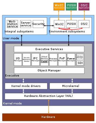
The architecture of Windows NT, a line of operating systems produced and sold by Microsoft, is a layered design that consists of two main components, user mode and kernel mode. It is a preemptive, reentrant multitasking operating system, which has been designed to work with uniprocessor and symmetrical multiprocessor (SMP)-based computers. To process input/output (I/O) requests, it uses packet-driven I/O, which utilizes I/O request packets (IRPs) and asynchronous I/O. Starting with Windows XP, Microsoft began making 64-bit versions of Windows available; before this, there were only 32-bit versions of these operating systems.
Memory type range registers (MTRRs) are a set of processor supplementary capability control registers that provide system software with control of how accesses to memory ranges by the CPU are cached. It uses a set of programmable model-specific registers (MSRs) which are special registers provided by most modern CPUs. Possible access modes to memory ranges can be uncached, write-through, write-combining, write-protect, and write-back. In write-back mode, writes are written to the CPU's cache and the cache is marked dirty, so that its contents are written to memory later.
In computing, the term 3 GB barrier refers to a limitation of some 32-bit operating systems running on x86 microprocessors. It prevents the operating systems from using all of 4 GiB (4 × 10243 bytes) of main memory. The exact barrier varies by motherboard and I/O device configuration, particularly the size of video RAM; it may be in the range of 2.75 GB to 3.5 GB. The barrier is not present with a 64-bit processor and 64-bit operating system, or with certain x86 hardware and an operating system such as Linux or certain versions of Windows Server and macOS that allow use of Physical Address Extension (PAE) mode on x86 to access more than 4 GiB of RAM.
A DMA attack is a type of side channel attack in computer security, in which an attacker can penetrate a computer or other device, by exploiting the presence of high-speed expansion ports that permit direct memory access (DMA).
This page is based on this Wikipedia article Text is available under the CC BY-SA 4.0 license; additional terms may apply. Images, videos and audio are available under their respective licenses.