The PowerPC 7xx is a family of third generation 32-bit PowerPC microprocessors designed and manufactured by IBM and Motorola. This family is called the PowerPC G3 by Apple Computer, which introduced it on November 10, 1997. The term "PowerPC G3" is often, and incorrectly, imagined to be a microprocessor when in fact a number of microprocessors from different vendors have been used. Such designations were applied to Mac computers such as the PowerBook G3, the multicolored iMacs, iBooks and several desktops, including both the Beige and Blue and White Power Macintosh G3s. The low power requirements and small size made the processors ideal for laptops and the name lived out its last days at Apple in the iBook.

The PowerPC 970, PowerPC 970FX, and PowerPC 970MP are 64-bit PowerPC processors from IBM introduced in 2002. When used in PowerPC-based Macintosh computers, Apple referred to them as the PowerPC G5.
PowerPC G4 is a designation formerly used by Apple and Eyetech to describe a fourth generation of 32-bit PowerPC microprocessors. Apple has applied this name to various processor models from Freescale, a former part of Motorola. Motorola and Freescale's proper name of this family of processors is PowerPC 74xx.

The POWER5 is a microprocessor developed and fabricated by IBM. It is an improved version of the POWER4. The principal improvements are support for simultaneous multithreading (SMT) and an on-die memory controller. The POWER5 is a dual-core microprocessor, with each core supporting one physical thread and two logical threads, for a total of two physical threads and four logical threads.
The POWER1 is a multi-chip CPU developed and fabricated by IBM that implemented the POWER instruction set architecture (ISA). It was originally known as the RISC System/6000 CPU or, when in an abbreviated form, the RS/6000 CPU, before introduction of successors required the original name to be replaced with one that used the same naming scheme (POWERn) as its successors in order to differentiate it from the newer designs.

POWER7 is a family of superscalar multi-core microprocessors based on the Power ISA 2.06 instruction set architecture released in 2010 that succeeded the POWER6 and POWER6+. POWER7 was developed by IBM at several sites including IBM's Rochester, MN; Austin, TX; Essex Junction, VT; T. J. Watson Research Center, NY; Bromont, QC and IBM Deutschland Research & Development GmbH, Böblingen, Germany laboratories. IBM announced servers based on POWER7 on 8 February 2010.
The PowerPC 400 family is a line of 32-bit embedded RISC processor cores based on the PowerPC or Power ISA instruction set architectures. The cores are designed to fit inside specialized applications ranging from system-on-a-chip (SoC) microcontrollers, network appliances, application-specific integrated circuits (ASICs) and field-programmable gate arrays (FPGAs) to set-top boxes, storage devices and supercomputers.

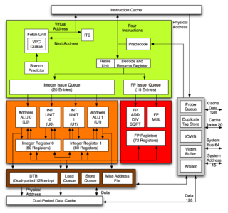
The POWER3 is a microprocessor, designed and exclusively manufactured by IBM, that implemented the 64-bit version of the PowerPC instruction set architecture (ISA), including all of the optional instructions of the ISA such as instructions present in the POWER2 version of the POWER ISA but not in the PowerPC ISA. It was introduced on 5 October 1998, debuting in the RS/6000 43P Model 260, a high-end graphics workstation. The POWER3 was originally supposed to be called the PowerPC 630 but was renamed, probably to differentiate the server-oriented POWER processors it replaced from the more consumer-oriented 32-bit PowerPCs. The POWER3 was the successor of the P2SC derivative of the POWER2 and completed IBM's long-delayed transition from POWER to PowerPC, which was originally scheduled to conclude in 1995. The POWER3 was used in IBM RS/6000 servers and workstations at 200 MHz. It competed with the Digital Equipment Corporation (DEC) Alpha 21264 and the Hewlett-Packard (HP) PA-8500.

The R10000, code-named "T5", is a RISC microprocessor implementation of the MIPS IV instruction set architecture (ISA) developed by MIPS Technologies, Inc. (MTI), then a division of Silicon Graphics, Inc. (SGI). The chief designers are Chris Rowen and Kenneth C. Yeager. The R10000 microarchitecture is known as ANDES, an abbreviation for Architecture with Non-sequential Dynamic Execution Scheduling. The R10000 largely replaces the R8000 in the high-end and the R4400 elsewhere. MTI was a fabless semiconductor company; the R10000 was fabricated by NEC and Toshiba. Previous fabricators of MIPS microprocessors such as Integrated Device Technology (IDT) and three others did not fabricate the R10000 as it was more expensive to do so than the R4000 and R4400.
The PowerPC 600 family was the first family of PowerPC processors built. They were designed at the Somerset facility in Austin, Texas, jointly funded and staffed by engineers from IBM and Motorola as a part of the AIM alliance. Somerset was opened in 1992 and its goal was to make the first PowerPC processor and then keep designing general purpose PowerPC processors for personal computers. The first incarnation became the PowerPC 601 in 1993, and the second generation soon followed with the PowerPC 603, PowerPC 604 and the 64-bit PowerPC 620.
The AMD Bulldozer Family 15h is a microprocessor microarchitecture for the FX and Opteron line of processors, developed by AMD for the desktop and server markets. Bulldozer is the codename for this family of microarchitectures. It was released on October 12, 2011, as the successor to the K10 microarchitecture.
The z10 is a microprocessor chip made by IBM for their System z10 mainframe computers, released February 26, 2008. It was called "z6" during development.
The Alpha 21264 is a Digital Equipment Corporation RISC microprocessor launched on 19 October 1998. The 21264 implemented the Alpha instruction set architecture (ISA).
The SPARC64 V (Zeus) is a SPARC V9 microprocessor designed by Fujitsu. The SPARC64 V was the basis for a series of successive processors designed for servers, and later, supercomputers.
The z196 microprocessor is a chip made by IBM for their zEnterprise 196 and zEnterprise 114 mainframe computers, announced on July 22, 2010. The processor was developed over a three-year time span by IBM engineers from Poughkeepsie, New York; Austin, Texas; and Böblingen, Germany at a cost of US$1.5 billion. Manufactured at IBM's Fishkill, New York fabrication plant, the processor began shipping on September 10, 2010. IBM stated that it was the world's fastest microprocessor at the time.

POWER8 is a family of superscalar multi-core microprocessors based on the Power ISA, announced in August 2013 at the Hot Chips conference. The designs are available for licensing under the OpenPOWER Foundation, which is the first time for such availability of IBM's highest-end processors.
The zEC12 microprocessor is a chip made by IBM for their zEnterprise EC12 and zEnterprise BC12 mainframe computers, announced on August 28, 2012. It is manufactured at the East Fishkill, New York fabrication plant. The processor began shipping in the fall of 2012. IBM stated that it was the world's fastest microprocessor and is about 25% faster than its predecessor the z196.

Espresso is the codename of the 32-bit central processing unit (CPU) used in Nintendo's Wii U video game console. It was designed by IBM, and was produced using a 45 nm silicon-on-insulator process. The Espresso chip resides together with a GPU from AMD on an MCM manufactured by Renesas. It was revealed at E3 2011 in June 2011 and released in November 2012.
IBM Power microprocessors are designed and sold by IBM for servers and supercomputers. The name "POWER" was originally presented as an acronym for "Performance Optimization With Enhanced RISC". The Power line of microprocessors has been used in IBM's RS/6000, AS/400, pSeries, iSeries, System p, System i, and Power Systems lines of servers and supercomputers. They have also been used in data storage devices and workstations by IBM and by other server manufacturers like Bull and Hitachi.
The AMD Jaguar Family 16h is a low-power microarchitecture designed by AMD. It is used in APUs succeeding the Bobcat Family microarchitecture in 2013 and being succeeded by AMD's Puma architecture in 2014. It is two-way superscalar and capable of out-of-order execution. It is used in AMD's Semi-Custom Business Unit as a design for custom processors and is used by AMD in four product families: Kabini aimed at notebooks and mini PCs, Temash aimed at tablets, Kyoto aimed at micro-servers, and the G-Series aimed at embedded applications. Both the PlayStation 4 and the Xbox One use chips based on the Jaguar microarchitecture, with more powerful GPUs than AMD sells in its own commercially available Jaguar APUs.


