Hyper-threading is Intel's proprietary simultaneous multithreading (SMT) implementation used to improve parallelization of computations performed on x86 microprocessors. It was introduced on Xeon server processors in February 2002 and on Pentium 4 desktop processors in November 2002. Since then, Intel has included this technology in Itanium, Atom, and Core 'i' Series CPUs, among others.
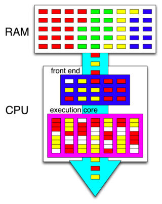
Simultaneous multithreading (SMT) is a technique for improving the overall efficiency of superscalar CPUs with hardware multithreading. SMT permits multiple independent threads of execution to better use the resources provided by modern processor architectures.
The POWER4 is a microprocessor developed by International Business Machines (IBM) that implemented the 64-bit PowerPC and PowerPC AS instruction set architectures. Released in 2001, the POWER4 succeeded the POWER3 and RS64 microprocessors, enabling RS/6000 and eServer iSeries models of AS/400 computer servers to run on the same processor, as a step toward converging the two lines. The POWER4 was a multicore microprocessor, with two cores on a single die, the first non-embedded microprocessor to do so. POWER4 Chip was first commercially available multiprocessor chip. The original POWER4 had a clock speed of 1.1 and 1.3 GHz, while an enhanced version, the POWER4+, reached a clock speed of 1.9 GHz. The PowerPC 970 is a derivative of the POWER4.

POWER7 is a family of superscalar multi-core microprocessors based on the Power ISA 2.06 instruction set architecture released in 2010 that succeeded the POWER6 and POWER6+. POWER7 was developed by IBM at several sites including IBM's Rochester, MN; Austin, TX; Essex Junction, VT; T. J. Watson Research Center, NY; Bromont, QC and IBM Deutschland Research & Development GmbH, Böblingen, Germany laboratories. IBM announced servers based on POWER7 on 8 February 2010.

The POWER6 is a microprocessor developed by IBM that implemented the Power ISA v.2.03. When it became available in systems in 2007, it succeeded the POWER5+ as IBM's flagship Power microprocessor. It is claimed to be part of the eCLipz project, said to have a goal of converging IBM's server hardware where practical.

The UltraSPARC IVJaguar and follow-up UltraSPARC IV+Panther are microprocessors designed by Sun Microsystems and manufactured by Texas Instruments. They are the fourth generation of UltraSPARC microprocessors, and implement the 64-bit SPARC V9 instruction set architecture (ISA). The UltraSPARC IV was originally to be succeeded by the UltraSPARC V Millennium, which was canceled after the announcement of the Niagara, now UltraSPARC T1 microprocessor in early 2004. It was instead succeeded by the Fujitsu-designed SPARC64 VI.
The AMD Bulldozer Family 15h is a microprocessor microarchitecture for the FX and Opteron line of processors, developed by AMD for the desktop and server markets. Bulldozer is the codename for this family of microarchitectures. It was released on October 12, 2011, as the successor to the K10 microarchitecture.
The z10 is a microprocessor chip made by IBM for their System z10 mainframe computers, released February 26, 2008. It was called "z6" during development.
The Alpha 21364, code-named "Marvel", also known as EV7 is a microprocessor developed by Digital Equipment Corporation (DEC), later Compaq Computer Corporation, that implemented the Alpha instruction set architecture (ISA).
The SPARC64 V (Zeus) is a SPARC V9 microprocessor designed by Fujitsu. The SPARC64 V was the basis for a series of successive processors designed for servers, and later, supercomputers.
The IBM A2 is an open source massively multicore capable and multithreaded 64-bit Power ISA processor core designed by IBM using the Power ISA v.2.06 specification. Versions of processors based on the A2 core range from a 2.3 GHz version with 16 cores consuming 65 W to a less powerful, four core version, consuming 20 W at 1.4 GHz.
The z196 microprocessor is a chip made by IBM for their zEnterprise 196 and zEnterprise 114 mainframe computers, announced on July 22, 2010. The processor was developed over a three-year time span by IBM engineers from Poughkeepsie, New York; Austin, Texas; and Böblingen, Germany at a cost of US$1.5 billion. Manufactured at IBM's Fishkill, New York fabrication plant, the processor began shipping on September 10, 2010. IBM stated that it was the world's fastest microprocessor at the time.

POWER8 is a family of superscalar multi-core microprocessors based on the Power ISA, announced in August 2013 at the Hot Chips conference. The designs are available for licensing under the OpenPOWER Foundation, which is the first time for such availability of IBM's highest-end processors.

Espresso is the codename of the 32-bit central processing unit (CPU) used in Nintendo's Wii U video game console. It was designed by IBM, and was produced using a 45 nm silicon-on-insulator process. The Espresso chip resides together with a GPU from AMD on an MCM manufactured by Renesas. It was revealed at E3 2011 in June 2011 and released in November 2012.
IBM Power microprocessors are designed and sold by IBM for servers and supercomputers. The name "POWER" was originally presented as an acronym for "Performance Optimization With Enhanced RISC". The Power line of microprocessors has been used in IBM's RS/6000, AS/400, pSeries, iSeries, System p, System i, and Power Systems lines of servers and supercomputers. They have also been used in data storage devices and workstations by IBM and by other server manufacturers like Bull and Hitachi.

POWER9 is a family of superscalar, multithreading, multi-core microprocessors produced by IBM, based on the Power ISA. It was announced in August 2016. The POWER9-based processors are being manufactured using a 14 nm FinFET process, in 12- and 24-core versions, for scale out and scale up applications, and possibly other variations, since the POWER9 architecture is open for licensing and modification by the OpenPOWER Foundation members.
The z13 is a microprocessor made by IBM for their z13 mainframe computers, announced on January 14, 2015. Manufactured at GlobalFoundries' East Fishkill, New York fabrication plant. IBM stated that it is the world's fastest microprocessor and is about 10% faster than its predecessor the zEC12 in general single-threaded computing, but significantly more when doing specialized tasks.
The z14 is a microprocessor made by IBM for their z14 mainframe computers, announced on July 17, 2017. Manufactured at GlobalFoundries' East Fishkill, New York fabrication plant. IBM stated that it is the world's fastest microprocessor by clock rate at 5.2 GHz, with a 10% increased performance per core and 30% for the whole chip compared to its predecessor the z13.
Power10 is a superscalar, multithreading, multi-core microprocessor family, based on the open source Power ISA, and announced in August 2020 at the Hot Chips conference; systems with Power10 CPUs. Generally available from September 2021 in the IBM Power10 Enterprise E1080 server.


