Memory controller

Last updated

A memory controller, also known as memory chip controller (MCC) or a memory controller unit (MCU), is a digital circuit that manages the flow of data going to and from a computer's main memory. [1] [2] When a memory controller is integrated into another chip, such as being placed on the same die or as an integral part of a microprocessor, it is usually called an integrated memory controller (IMC).

Contents

Memory controllers contain the logic necessary to read and write to dynamic random-access memory (DRAM), and to refresh the DRAM in order to prevent losing data written to it, as otherwise the capacitors leak their charge within not more than 64 milliseconds. Reading and writing to DRAM is performed by selecting the row and column data addresses of the DRAM as the inputs to the multiplexer circuit, where the demultiplexer on the DRAM uses the converted inputs to select the correct memory location and return the data, which is then passed back through a multiplexer to consolidate the data in order to reduce the required bus width for the operation. Memory controllers' bus widths range from 8-bit in earlier systems, to 512-bit in more complicated systems, where they are typically implemented as four 64-bit simultaneous memory controllers operating in parallel, though some operate with two 64-bit memory controllers being used to access a 128-bit memory device.

Some memory controllers, such as the one integrated into PowerQUICC II processors, include error detection and correction hardware. [3] A common form of memory controller is the memory management unit (MMU), which in many operating systems implements virtual addressing.

History

Older Intel and PowerPC-based computers have memory controller chips that are separate from the main processor. Often these are integrated into the northbridge of the computer, also sometimes called a memory controller hub.

Most modern desktop or workstation microprocessors use an integrated memory controller (IMC), including microprocessors from Intel, AMD, and those built around the ARM architecture.

Prior to K8 (circa 2003), AMD microprocessors had a memory controller implemented on their motherboard's northbridge. In K8 and later, AMD employed an integrated memory controller. [4] Likewise, until Nehalem (circa 2008), Intel microprocessors used memory controllers implemented on the motherboard's northbridge. Nehalem and later switched to an integrated memory controller. [5]

Other examples of microprocessor architectures that use integrated memory controllers include NVIDIA's Fermi, IBM's POWER5, and Sun Microsystems's UltraSPARC T1.

While an integrated memory controller has the potential to increase the system's performance, such as by reducing memory latency, it locks the microprocessor to a specific type (or types) of memory, forcing a redesign in order to support newer memory technologies. When DDR2 SDRAM was introduced, AMD released new Athlon 64 CPUs. These new models, with a DDR2 controller, use a different physical socket (known as Socket AM2), so that they will only fit in motherboards designed for the new type of RAM. When the memory controller is not on-die, the same CPU may be installed on a new motherboard, with an updated northbridge.

Some microprocessors in the 1990s, such as the DEC Alpha 21066 and HP PA-7300LC, had integrated memory controllers; however, rather than for performance gains, this was implemented to reduce the cost of systems by eliminating the need for an external memory controller.

Some CPUs are designed to have their memory controllers as dedicated external components that are not part of the chipset. An example is IBM POWER8, which uses external Centaur chips that are mounted onto DIMM modules and act as memory buffers, L4 cache chips, and as the actual memory controllers. The first version of the Centaur chip used DDR3 memory but an updated version was later released which can use DDR4. [6]

Security

A few experimental memory controllers (mostly aimed at the server market where data protection is legally required) contain a second level of address translation, in addition to the first level of address translation performed by the CPU's memory management unit. [7]

Memory controllers integrated into certain Intel Core processors also provide memory scrambling as a feature that turns user data written to the main memory into pseudo-random patterns. [8] [9]

Memory Scrambling (in Cryptographic Theory) is supposed to prevent forensic and reverse-engineering analysis based on DRAM data remanence by effectively rendering various types of cold boot attacks ineffective. In current practice this has not been achieved.

However Memory Scrambling has only been designed to address DRAM-related electrical problems. The late 2010s Memory Scrambling Standards do not fix or prevent security issues or problems. The 2010s Memory Scrambling standards are not cryptographically secure, or necessarily open sourced or open to public revision or analysis. [10]

ASUS and Intel have their own memory scrambling standards. Currently ASUS motherboards have allowed the user to choose which memory scrambling standards to use [ASUS or Intel] or whether to turn the feature off entirely.

Variants

Double data rate memory

Double data rate (DDR) memory controllers are used to drive DDR SDRAM, where data is transferred on both rising and falling edges of the system's memory clock. DDR memory controllers are significantly more complicated when compared to single data rate controllers [ citation needed ], but they allow for twice the data to be transferred without increasing the memory cell's clock rate or bus width.

Multichannel memory

Multichannel memory memory controllers are memory controllers where the DRAM devices are separated on to multiple different buses to allow the memory controller(s) to access them in parallel. This increases the theoretical amount of bandwidth of the bus by a factor of the number of channels. While a channel for every DRAM cell would be the ideal solution, adding more channels is very difficult due to wire count, line capacitance, and the need for parallel access lines to have identical lengths.

Fully buffered memory

Fully buffered memory systems place a memory buffer device on every memory module (called an FB-DIMM when Fully Buffered RAM is used), which unlike traditional memory controller devices, use a serial data link to the memory controller instead of the parallel link used in previous RAM designs. This decreases the number of the wires necessary to place the memory devices on a motherboard (allowing for a smaller number of layers to be used, meaning more memory devices can be placed on a single board), at the expense of increasing latency (the time necessary to access a memory location). This increase is due to the time required to convert the parallel information read from the DRAM cell to the serial format used by the FB-DIMM controller, and back to a parallel form in the memory controller on the motherboard.

In theory, the FB-DIMM's memory buffer device could be built to access any DRAM cells, allowing for memory cell agnostic memory controller design, but this has not been demonstrated, as the technology is in its infancy.

Flash memory controller

Many flash memory devices, such as USB flash drives and solid state drives, include a flash memory controller. Flash memory is inherently slower to access than RAM and often becomes unusable after a few million write cycles, which generally makes it unsuitable for RAM applications.

See also

Related Research Articles

<span class="mw-page-title-main">DDR SDRAM</span> Type of computer memory

Double Data Rate Synchronous Dynamic Random-Access Memory is a double data rate (DDR) synchronous dynamic random-access memory (SDRAM) class of memory integrated circuits used in computers. DDR SDRAM, also retroactively called DDR1 SDRAM, has been superseded by DDR2 SDRAM, DDR3 SDRAM, DDR4 SDRAM and DDR5 SDRAM. None of its successors are forward or backward compatible with DDR1 SDRAM, meaning DDR2, DDR3, DDR4 and DDR5 memory modules will not work on DDR1-equipped motherboards, and vice versa.

<span class="mw-page-title-main">DIMM</span> Computer memory module

A DIMM, or Dual In-Line Memory Module, is a popular type of memory module used in computers. It is a printed circuit board with one or both sides holding DRAM chips and pins. The vast majority of DIMMs are standardized through JEDEC standards, although there are proprietary DIMMs. DIMMs come in a variety of speeds and sizes, but generally are one of two lengths - PC which are 133.35 mm (5.25 in) and laptop (SO-DIMM) which are about half the size at 67.60 mm (2.66 in).

HyperTransport (HT), formerly known as Lightning Data Transport, is a technology for interconnection of computer processors. It is a bidirectional serial/parallel high-bandwidth, low-latency point-to-point link that was introduced on April 2, 2001. The HyperTransport Consortium is in charge of promoting and developing HyperTransport technology.

<span class="mw-page-title-main">Chipset</span> Electronic component to manage data flow of a CPU

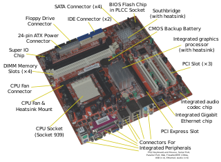
In a computer system, a chipset is a set of electronic components on one or more integrated circuits that manages the data flow between the processor, memory and peripherals. The chipset is usually found on the motherboard of computers. Chipsets are usually designed to work with a specific family of microprocessors. Because it controls communications between the processor and external devices, the chipset plays a crucial role in determining system performance.

<span class="mw-page-title-main">Northbridge (computing)</span> PC chip handling onboard control tasks

In computing, a northbridge is a microchip that comprises the core logic chipset architecture on motherboards to handle high-performance tasks, especially for older personal computers. It is connected directly to a CPU via the front-side bus (FSB), and is usually used in conjunction with a slower southbridge to manage communication between the CPU and other parts of the motherboard.

<span class="mw-page-title-main">Southbridge (computing)</span> One of the two chips in the core logic chipset architecture on a PC motherboard

The southbridge is one of the two chips in the core logic chipset on older personal computer (PC) motherboards, the other being the northbridge. As of 2023, most personal computer devices no longer use a set of two chips, and instead have a single chip acting as the 'chipset', for example Intel's Z790 chipset.

<span class="mw-page-title-main">Double data rate</span> Method of computer bus operation

In computing, double data rate (DDR) describes a computer bus that transfers data on both the rising and falling edges of the clock signal and hence doubles the memory bandwidth by transferring data twice per clock cycle. This is also known as double pumped, dual-pumped, and double transition. The term toggle mode is used in the context of NAND flash memory.

<span class="mw-page-title-main">Geode (processor)</span> Series of x86-compatible processor

Geode was a series of x86-compatible system-on-a-chip (SoC) microprocessors and I/O companions produced by AMD, targeted at the embedded computing market.

The Intel QuickPath Interconnect (QPI) is a point-to-point processor interconnect developed by Intel which replaced the front-side bus (FSB) in Xeon, Itanium, and certain desktop platforms starting in 2008. It increased the scalability and available bandwidth. Prior to the name's announcement, Intel referred to it as Common System Interface (CSI). Earlier incarnations were known as Yet Another Protocol (YAP) and YAP+.

In the fields of digital electronics and computer hardware, multi-channel memory architecture is a technology that increases the data transfer rate between the DRAM memory and the memory controller by adding more channels of communication between them. Theoretically, this multiplies the data rate by exactly the number of channels present. Dual-channel memory employs two channels. The technique goes back as far as the 1960s having been used in IBM System/360 Model 91 and in CDC 6600.

Registered memory is computer memory that has a register between the DRAM modules and the system's memory controller. A registered memory module places less electrical load on a memory controller compared to an unregistered one. Registered memory allows a computer system to remain stable with a higher number of memory modules than it would have otherwise.

Double Data Rate 3 Synchronous Dynamic Random-Access Memory is a type of synchronous dynamic random-access memory (SDRAM) with a high bandwidth interface, and has been in use since 2007. It is the higher-speed successor to DDR and DDR2 and predecessor to DDR4 synchronous dynamic random-access memory (SDRAM) chips. DDR3 SDRAM is neither forward nor backward compatible with any earlier type of random-access memory (RAM) because of different signaling voltages, timings, and other factors.

<span class="mw-page-title-main">Fully Buffered DIMM</span>

A Fully Buffered DIMM (FB-DIMM) is a type of memory module used in computer systems. It is designed to improve memory performance and capacity by allowing multiple memory modules to be each connected to the memory controller using a serial interface, rather than a parallel one. Unlike the parallel bus architecture of traditional DRAMs, an FB-DIMM has a serial interface between the memory controller and the advanced memory buffer (AMB). Conventionally, data lines from the memory controller have to be connected to data lines in every DRAM module, i.e. via multidrop buses. As the memory width increases together with the access speed, the signal degrades at the interface between the bus and the device. This limits the speed and memory density, so FB-DIMMs take a different approach to solve the problem.

<span class="mw-page-title-main">ECC memory</span> Self-correcting computer data storage

Error correction code memory is a type of computer data storage that uses an error correction code (ECC) to detect and correct n-bit data corruption which occurs in memory.

The Socket G3 Memory Extender (G3MX) was a planned Advanced Micro Devices' solution to the problem of connecting large amounts of memory to a single microprocessor. The G3MX was expected to be available on AMD 800S series chipset for server market starting from 2009, but was officially cancelled together with the cancellation of Socket G3 in early 2008.

<span class="mw-page-title-main">Platform Controller Hub</span> Family of Intels single-chip chipsets

The Platform Controller Hub (PCH) is a family of Intel's single-chip chipsets, first introduced in 2009. It is the successor to the Intel Hub Architecture, which used two chips–a northbridge and southbridge, and first appeared in the Intel 5 Series.

Bloomfield is the code name for Intel high-end desktop processors sold as Core i7-9xx and single-processor servers sold as Xeon 35xx., in almost identical configurations, replacing the earlier Yorkfield processors. The Bloomfield core is closely related to the dual-processor Gainestown, which has the same CPUID value of 0106Ax and which uses the same socket. Bloomfield uses a different socket than the later Lynnfield and Clarksfield processors based on the same 45 nm Nehalem microarchitecture, even though some of these share the same Intel Core i7 brand.

<span class="mw-page-title-main">GPU switching</span> Mechanism for computers with multiple graphic controllers

GPU switching is a mechanism used on computers with multiple graphic controllers. This mechanism allows the user to either maximize the graphic performance or prolong battery life by switching between the graphic cards. It is mostly used on gaming laptops which usually have an integrated graphic device and a discrete video card.

Apollo VP3 is a x86 based Socket 7 chipset which was manufactured by VIA Technologies and was launched in 1997. On its time Apollo VP3 was a high performance, cost effective, and energy efficient chipset. It offered AGP support for Socket 7 processors which was not supported at that moment by Intel, SiS and ALi chipsets. In November 1997 FIC released motherboard PA-2012, which uses Apollo VP3 and has AGP bus. This was the first Socket 7 motherboard supporting AGP.

References

  1. Comptia A+ Certification Exam Guide, Seventh Edition, by Mike Meyers, in the glossary, bottom of page 1278: "Chip that handles memory requests from the CPU."
  2. Neat, Adam G. (2003-12-04). Maximizing Performance and Scalability with IBM WebSphere. Apress. ISBN   9781590591307 . Retrieved 6 February 2015.
  3. "Memory Controller"
  4. Vries, Hans de. "Chip Architect: AMD's Next Generation Micro Processor's Architecture". www.chip-architect.com. Retrieved 2018-03-17.
  5. Torres, Gabriel (2008-08-26). "Inside Intel Nehalem Microarchitecture". Hardware Secrets. p. 2. Retrieved 7 September 2017.
  6. Prickett Morgan, Timothy (2016-10-17). "IBM Brings DDR4 Memory To Bear On Power Systems". IT Jungle. p. 1. Retrieved 2017-09-07.
  7. This is a security feature in that it allows the Operating System to provide better protection separate from using a bit to deny arbitrary code execution in (System and/or User) RAM memory areas. John Carter, Wilson Hsieh, Leigh Stoller, Mark Swansony, Lixin Zhang, et al. "Impulse: Building a Smarter Memory Controller".
  8. "2nd Generation Intel Core Processor Family Desktop, Intel Pentium Processor Family Desktop, and Intel Celeron Processor Family Desktop" (PDF). June 2013. p. 23. Retrieved 2015-11-03.
  9. "2nd Generation Intel Core Processor Family Mobile and Intel Celeron Processor Family Mobile" (PDF). September 2012. p. 24. Retrieved 2015-11-03.
  10. Igor Skochinsky (2014-03-12). "Secret of Intel Management Engine". SlideShare. pp. 26–29. Retrieved 2014-07-13.