Two types of DIMMs: a 168-pin SDRAM module (top) and a 184-pin DDR SDRAM module (bottom). The SDRAM module has two notches (rectangular cuts or incisions) on the bottom edge, while the DDR1 SDRAM module has one. Also, each module has eight RAM chips, but the lower one has an unoccupied space for the ninth chip; this space is occupied in ECC DIMMs.Three SDRAM DIMM slots on a ABIT BP6 computer motherboard
A DIMM, or Dual In-Line Memory Module, is a popular type of memory module used in computers. It is a printed circuit board with one or both sides (front and back) holding DRAMchips and pins.[1] The vast majority of DIMMs are standardized through JEDEC standards, although there are proprietary DIMMs. DIMMs come in a variety of speeds and sizes, but generally are one of two lengths - PC which are 133.35mm (5.25in) and laptop (SO-DIMM) which are about half the size at 67.60mm (2.66in).[2]
DIMMs (Dual In-line Memory Module) were a 1990s upgrade for SIMMs (Single In-line Memory Modules)[3][4] as IntelP5-based Pentium processors began to gain market share. The Pentium had a 64-bit bus width, which would require SIMMs installed in matched pairs in order to populate the data bus. The processor would then access the two SIMMs in parallel.
DIMMs were introduced to eliminate this disadvantage. The contacts on SIMMs on both sides are redundant, while DIMMs have separate electrical contacts on each side of the module.[5] This allowed them to double the SIMMs 32-bit data path into a 64-bit data path.[6]
The name "DIMM" was chosen as an acronym for Dual In-line Memory Module symbolizing the split in the contacts of a SIMM into two independent rows.[6] Many enhancements have occurred to the modules in the intervening years, but the word "DIMM" has remained as one of the generic terms for a computer memory module.
Variants
There are numerous DIMM variants, employing different pin-counts:
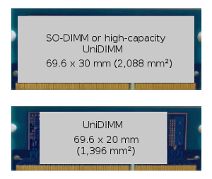
A 200-pin PC2-5300 DDR2 SO-DIMMA 204-pin PC3-10600 DDR3 SO-DIMMA SO-DIMM slot on a computer motherboard
A SO-DIMM (pronounced "so-dimm" /ˈsoʊdɪm/, also spelled "SODIMM") or small outline DIMM, is a smaller alternative to a DIMM, being roughly half the physical size of a regular DIMM. The first SODIMMs had 72 pins and were introduced by JEDEC in 1997.[8][9][10] Before its introduction, many laptops would use proprietary[11] RAM modules which were expensive and hard to find.[8][12]
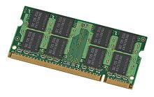
SO-DIMMs are often used in computers that have limited space, which include laptops, notebooks, small-footprint personal computers such as those based on Nano-ITXmotherboards, high-end upgradable office printers, and networking hardware such as routers and NAS devices.[13] They are usually available with the same size data path and speed ratings of the regular DIMMs though normally with smaller capacities.
SDR 168-pin SDRAM
Notch positions on DDR (top) and DDR2 (bottom) DIMM modules
On the bottom edge of 168-pin DIMMs there are two notches, and the location of each notch determines a particular feature of the module. The first notch is the DRAM key position, which represents RFU (reserved future use), registered, and unbuffered DIMM types (left, middle and right position, respectively). The second notch is the voltage key position, which represents 5.0V, 3.3V, and RFU DIMM types (order is the same as above).
DDR, DDR2, DDR3, DDR4 and DDR5 all have different pin counts and/or different notch positions, and none of them are forward compatible or backward compatible. DDR5 SDRAM is the most recent type of DDR memory and has been in use since 2020.
SPD EEPROM
A DIMM's capacity and other operational parameters may be identified with serial presence detect (SPD), an additional chip which contains information about the module type and timing for the memory controller to be configured correctly. The SPD EEPROM connects to the System Management Bus and may also contain thermal sensors (TS-on-DIMM).[14]
Error correction
ECC DIMMs are those that have extra data bits which can be used by the system memory controller to detect and correct errors. There are numerous ECC schemes, but perhaps the most common is Single Error Correct, Double Error Detect (SECDED) which uses an extra byte per 64-bit word. ECC modules usually carry a multiple of 9 instead of a multiple of 8 chips.
Sometimes memory modules are designed with two or more independent sets of DRAM chips connected to the same address and data buses; each such set is called a rank. Ranks that share the same slot, only one rank may be accessed at any given time; it is specified by activating the corresponding rank's chip select (CS) signal. The other ranks on the module are deactivated for the duration of the operation by having their corresponding CS signals deactivated. DIMMs are currently being commonly manufactured with up to four ranks per module. Consumer DIMM vendors have recently begun to distinguish between single and dual ranked DIMMs.
After a memory word is fetched, the memory is typically inaccessible for an extended period of time while the sense amplifiers are charged for access of the next cell. By interleaving the memory (e.g. cells 0, 4, 8, etc. are stored together in one rank), sequential memory accesses can be performed more rapidly because sense amplifiers have 3 cycles of idle time for recharging, between accesses.
DIMMs are often referred to as "single-sided" or "double-sided" to describe whether the DRAM chips are located on one or both sides of the module's printed circuit board (PCB). However, these terms may cause confusion, as the physical layout of the chips does not necessarily relate to how they are logically organized or accessed.
JEDEC decided that the terms "dual-sided", "double-sided", or "dual-banked" were not correct when applied to registered DIMMs (RDIMMs).
Organization
Most DIMMs are built using "×4" ("by four") or "×8" ("by eight") memory chips with up to nine chips per side; "×4" and "×8" refer to the data width of the DRAM chips in bits. High capacity DIMMs such as 256GB DIMMs can have up to 19 chips per side.
In the case of "×4" registered DIMMs, the data width per side is 36 bits; therefore, the memory controller (which requires 72 bits) needs to address both sides at the same time to read or write the data it needs. In this case, the two-sided module is single-ranked. For "×8" registered DIMMs, each side is 72 bits wide, so the memory controller only addresses one side at a time (the two-sided module is dual-ranked).
The above example applies to ECC memory that stores 72 bits instead of the more common 64. There would also be one extra chip per group of eight, which is not counted.
Speeds
For various technologies, there are certain bus and device clock frequencies that are standardized; there is also a decided nomenclature for each of these speeds for each type.
DIMMs based on Single Data Rate (SDR) DRAM have the same bus frequency for data, address and control lines. DIMMs based on Double Data Rate (DDR) DRAM have data but not the strobe at double the rate of the clock; this is achieved by clocking on both the rising and falling edge of the data strobes. Power consumption and voltage gradually became lower with each generation of DDR-based DIMMs.
Another influence is Column Access Strobe (CAS) latency, or CL which affects memory access speed. This is the delay time between the READ command and the moment data is available. See main article CAS/CL.
A comparison between 200-pin DDR and DDR2 SDRAM SO-DIMMs, and a 204-pin DDR3 SO-DIMM module
Several form factors are commonly used in DIMMs. Single Data Rate Synchronous DRAM (SDR SDRAM) DIMMs were primarily manufactured in 1.5 inches (38mm) and 1.7 inches (43mm) heights. When 1U rackmount servers started becoming popular, these form factor registered DIMMs had to plug into angled DIMM sockets to fit in the 1.75 inches (44mm) high box. To alleviate this issue, the next standards of DDR DIMMs were created with a "low profile" (LP) height of around 1.2 inches (30mm). These fit into vertical DIMM sockets for a 1U platform.
With the advent of blade servers, angled slots have once again become common in order to accommodate LP form factor DIMMs in these space-constrained boxes. This led to the development of the Very Low Profile (VLP) form factor DIMM with a height of around 0.72 inches (18mm). The DDR3 JEDEC standard for VLP DIMM height is around 0.740 inches (18.8mm). These will fit vertically in ATCA systems.
Full-height 240-pin DDR2 and DDR3 DIMMs are all specified at a height of around 1.18 inches (30mm) by standards set by JEDEC. These form factors include 240-pin DIMM, SO-DIMM, Mini-DIMM and Micro-DIMM.[16]
Full-height 288-pin DDR4 DIMMs are slightly taller than their DDR3 counterparts at 1.23 inches (31mm). Similarly, VLP DDR4 DIMMs are also marginally taller than their DDR3 equivalent at nearly 0.74 inches (19mm).[17]
As of Q2 2017, Asus has had a PCI-E based "DIMM.2", which has a similar socket to DDR3 DIMMs and is used to put in a module to connect up to two M.2NVMe solid-state drives. However, it cannot use common DDR type ram and does not have much support other than Asus.[18]
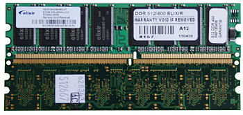
Regular DIMMs are generally 133.35mm in length, SO-DIMMs 67.6mm.[2]
Double Data Rate Synchronous Dynamic Random-Access Memory is a double data rate (DDR) synchronous dynamic random-access memory (SDRAM) class of memory integrated circuits used in computers. DDR SDRAM, also retroactively called DDR1 SDRAM, has been superseded by DDR2 SDRAM, DDR3 SDRAM, DDR4 SDRAM and DDR5 SDRAM. None of its successors are forward or backward compatible with DDR1 SDRAM, meaning DDR2, DDR3, DDR4 and DDR5 memory modules will not work on DDR1-equipped motherboards, and vice versa.
Synchronous dynamic random-access memory is any DRAM where the operation of its external pin interface is coordinated by an externally supplied clock signal.
Rambus DRAM (RDRAM), and its successors Concurrent Rambus DRAM (CRDRAM) and Direct Rambus DRAM (DRDRAM), are types of synchronous dynamic random-access memory (SDRAM) developed by Rambus from the 1990s through to the early 2000s. The third-generation of Rambus DRAM, DRDRAM was replaced by XDR DRAM. Rambus DRAM was developed for high-bandwidth applications and was positioned by Rambus as replacement for various types of contemporary memories, such as SDRAM.
Double Data Rate 2 Synchronous Dynamic Random-Access Memory is a double data rate (DDR) synchronous dynamic random-access memory (SDRAM) interface. It is a JEDEC standard (JESD79-2); first published in September 2003. DDR2 succeeded the original DDR SDRAM specification, and was itself succeeded by DDR3 SDRAM in 2007. DDR2 DIMMs are neither forward compatible with DDR3 nor backward compatible with DDR.
In computing, double data rate (DDR) describes a computer bus that transfers data on both the rising and falling edges of the clock signal and hence doubles the memory bandwidth by transferring data twice per clock cycle. This is also known as double pumped, dual-pumped, and double transition. The term toggle mode is used in the context of NAND flash memory.
In the fields of digital electronics and computer hardware, multi-channel memory architecture is a technology that increases the data transfer rate between the DRAM memory and the memory controller by adding more channels of communication between them. Theoretically, this multiplies the data rate by exactly the number of channels present. Dual-channel memory employs two channels. The technique goes back as far as the 1960s having been used in IBM System/360 Model 91 and in CDC 6600.
In computing, serial presence detect (SPD) is a standardized way to automatically access information about a memory module. Earlier 72-pin SIMMs included five pins that provided five bits of parallel presence detect (PPD) data, but the 168-pin DIMM standard changed to a serial presence detect to encode more information.
Double Data Rate 3 Synchronous Dynamic Random-Access Memory is a type of synchronous dynamic random-access memory (SDRAM) with a high bandwidth interface, and has been in use since 2007. It is the higher-speed successor to DDR and DDR2 and predecessor to DDR4 synchronous dynamic random-access memory (SDRAM) chips. DDR3 SDRAM is neither forward nor backward compatible with any earlier type of random-access memory (RAM) because of different signaling voltages, timings, and other factors.
A Fully Buffered DIMM (FB-DIMM) is a type of memory module used in computer systems. It is designed to improve memory performance and capacity by allowing multiple memory modules to be each connected to the memory controller using a serial interface, rather than a parallel one. Unlike the parallel bus architecture of traditional DRAMs, an FB-DIMM has a serial interface between the memory controller and the advanced memory buffer (AMB). Conventionally, data lines from the memory controller have to be connected to data lines in every DRAM module, i.e. via multidrop buses. As the memory width increases together with the access speed, the signal degrades at the interface between the bus and the device. This limits the speed and memory density, so FB-DIMMs take a different approach to solve the problem.
GDDR4 SDRAM, an abbreviation for Graphics Double Data Rate 4 Synchronous Dynamic Random-Access Memory, is a type of graphics card memory (SGRAM) specified by the JEDEC Semiconductor Memory Standard. It is a rival medium to Rambus's XDR DRAM. GDDR4 is based on DDR3 SDRAM technology and was intended to replace the DDR2-based GDDR3, but it ended up being replaced by GDDR5 within a year.
A memory controller, also known as memory chip controller (MCC) or a memory controller unit (MCU), is a digital circuit that manages the flow of data going to and from a computer's main memory. When a memory controller is integrated into another chip, such as being placed on the same die or as an integral part of a microprocessor, it is usually called an integrated memory controller (IMC).
In computing, a memory module or RAM stick is a printed circuit board on which memory integrated circuits are mounted.
The JEDEC memory standards are the specifications for semiconductor memory circuits and similar storage devices promulgated by the Joint Electron Device Engineering Council (JEDEC) Solid State Technology Association, a semiconductor trade and engineering standardization organization.
Double Data Rate 4 Synchronous Dynamic Random-Access Memory is a type of synchronous dynamic random-access memory with a high bandwidth interface.
Low-Power Double Data Rate (LPDDR), also known as LPDDR SDRAM, is a type of synchronous dynamic random-access memory that consumes less power and is targeted for mobile computers and devices such as mobile phones. Older variants are also known as Mobile DDR, and abbreviated as mDDR.
A memory rank is a set of DRAM chips connected to the same chip select, which are therefore accessed simultaneously. In practice all DRAM chips share all of the other command and control signals, and only the chip select pins for each rank are separate.
GDDR3 SDRAM is a type of DDR SDRAM specialized for graphics processing units (GPUs) offering less access latency and greater device bandwidths. Its specification was developed by ATI Technologies in collaboration with DRAM vendors including Elpida Memory, Hynix Semiconductor, Infineon and Micron. It was later adopted as a JEDEC standard.
HyperCloud Memory (HCDIMM) is a DDR3 SDRAM dual in-line memory module (DIMM) used in server applications requiring a great deal of memory. It was initially launched in 2009 at the International Supercomputing Conference by Irvine, California, based company, Netlist Inc. It was never a JEDEC standard, and the main server vendors supporting it were IBM and Hewlett Packard Enterprise.
Double Data Rate 5 Synchronous Dynamic Random-Access Memory is the latest type of synchronous dynamic random-access memory. Compared to its predecessor DDR4 SDRAM, DDR5 was planned to reduce power consumption, while doubling bandwidth. The standard, originally targeted for 2018, was released on July 14, 2020.
UniDIMM is a specification for dual in-line memory modules (DIMMs), which are printed circuit boards (PCBs) designed to carry dynamic random-access memory (DRAM) chips. UniDIMMs can be populated with either DDR3 or DDR4 chips, with no support for any additional memory control logic; as a result, the computer's memory controller must support both DDR3 and DDR4 memory standards. The UniDIMM specification was created by Intel for its Skylake microarchitecture, whose integrated memory controller (IMC) supports both DDR3 and DDR4 memory technologies.
References
↑ "What is DIMM(Dual Inline Memory Module)?". GeeksforGeeks. 2020-04-15. Retrieved 2024-04-07. In the case of SIMM, the connectors are only present on the single side of the module...DIMM has a row of connectors on both sides(front and back) of the module
This page is based on this Wikipedia article Text is available under the CC BY-SA 4.0 license; additional terms may apply. Images, videos and audio are available under their respective licenses.