XDR DRAM

Last updated
XDR DRAM. XDRAM.jpg
XDR DRAM.

XDR DRAM (extreme data rate dynamic random-access memory) is a high-performance dynamic random-access memory interface. It is based on and succeeds RDRAM. Competing technologies include DDR2 and GDDR4.

Contents

Overview

XDR was designed to be effective in small, high-bandwidth consumer systems, high-performance memory applications, and high-end GPUs. It eliminates the unusually high latency problems that plagued early forms of RDRAM. Also, XDR DRAM has heavy emphasis on per-pin bandwidth, which can benefit further cost control on PCB production. This is because fewer lanes are needed for the same amount of bandwidth. Rambus owns the rights to the technology. XDR is used by Sony in the PlayStation 3 console. [1]

Technical specifications

Performance

Features

Power requirements

Ease of system design

Latency

Protocol

An XDR RAM chip's high-speed signals are a differential clock input (clock from master, CFM/CFMN), a 12-bit single-ended request/command bus (RQ11..0), and a bidirectional differential data bus up to 16 bits wide (DQ15..0/DQN15..0). The request bus may be connected to several memory chips in parallel, but the data bus is point to point; only one RAM chip may be connected to it. To support different amounts of memory with a fixed-width memory controller, the chips have a programmable interface width. A 32-bit-wide DRAM controller may support 2 16-bit chips, or be connected to 4 memory chips each of which supplies 8 bits of data, or up to 16 chips configured with 2-bit interfaces.

In addition, each chip has a low-speed serial bus used to determine its capabilities and configure its interface. This consists of three shared inputs: a reset line (RST), a serial command input (CMD) and a serial clock (SCK), and serial data in/out lines (SDI and SDO) that are daisy-chained together and eventually connect to a single pin on the memory controller.

All single-ended lines are active-low; an asserted signal or logical 1 is represented by a low voltage.

The request bus operates at double data rate relative to the clock input. Two consecutive 12-bit transfers (beginning with the falling edge of CFM) make a 24-bit command packet.

The data bus operates at 8x the speed of the clock; a 400 MHz clock generates 3200 MT/s. All data reads and writes operate in 16-transfer bursts lasting 2 clock cycles.

Request packet formats are as follows:

XDR DRAM request packet formats [3]
Clock
edge
BitNOPColumn read/writeCalibrate/power-downPrecharge/refreshRow ActivateMasked write
BitBitDescriptionBitDescriptionBitDescriptionBitDescriptionBitDescription
RQ1100COL opcode0COLX opcode0ROWP opcode0ROWA opcode1COLM opcode
RQ1000001M3Write mask
low bits
RQ90011R9Row address
high bits
M2
RQ80101R10M1
RQ7xWRXWrite/Read bitxreservedPOP1Precharge delay (0–3)R11M0
RQ6xC8Column address
high bits
xPOP0R12reservedC8Column address
high bits
RQ5xC9xxreservedR13C9
RQ4xC10reservedxxR14C10reserved
RQ3xC11XOP3SubopcodexR15C11
RQ2xBC2Bank addressXOP2BP2Precharge bankBA2Bank addressBC2Bank address
RQ1xBC1XOP1BP1BA1BC1
RQ0xBC0XOP0BP0BA0BC0
RQ11xDELCCommand delay (0–1)xreservedPOP2Precharge enableDELACommand delay (0–1)M7Write mask
high bits
RQ10xxreservedxROP2Refresh commandR8Row address
low bits
M6
RQ9xxxROP1R7M5
RQ8xxxROP0R6M4
RQ7xC7Column address
low bits
xDELR1Refresh delay (0–3)R5C7Column address
low bits
RQ6xC6xDELR0R4C6
RQ5xC5xxreservedR3C5
RQ4xC4xxR2C4
RQ3xSC3Sub-column addressxxR1SC3Sub-column address
RQ2xSC2xBR2Refresh bankR0SC2
RQ1xSC1xBR1SR1Sub-row addressSC1
RQ0xSC0xBR0SR0SC0

There are a large number of timing constraints giving minimum times that must elapse between various commands (see Dynamic random-access memory § Memory timing); the DRAM controller sending them must ensure they are all met.

Some commands contain delay fields; these delay the effect of that command by the given number of clock cycles. This permits multiple commands (to different banks) to take effect on the same clock cycle.

Row activate command

This operates equivalently to standard SDRAM's activate command, specifying a row address to be loaded into the bank's sense amplifier array. To save power, a chip may be configured to only activate a portion of the sense amplifier array. In this case, the SR1..0 bits specify the half or quarter of the row to activate, and following read/write commands' column addresses are required to be limited to that portion. (Refresh operations always use the full row.)

Read/write commands

These operate analogously to a standard SDRAM's read or write commands, specifying a column address. Data is provided to the chip a few cycles after a write command (typically 3), and is output by the chip several cycles after a read command (typically 6). Just as with other forms of SDRAM, the DRAM controller is responsible for ensuring that the data bus is not scheduled for use in both directions at the same time. Data is always transferred in 16-transfer bursts, lasting 2 clock cycles. Thus, for a ×16 device, 256 bits (32 bytes) are transferred per burst.

If the chip is using a data bus less than 16 bits wide, one or more of the sub-column address bits are used to select the portion of the column to be presented on the data bus. If the data bus is 8 bits wide, SC3 is used to identify which half of the read data to access; if the data bus is 4 bits wide, SC3 and SC2 are used, etc.

Unlike conventional SDRAM, there is no provision for choosing the order in which the data is supplied within a burst. Thus, it is not possible to perform critical-word-first reads.

Masked write command

The masked write command is similar to a normal write, but no command delay is permitted and a mask byte is supplied. This permits controlling which 8-bit fields are written. This is not a bitmap indicating which bytes are to be written; it would not be large enough for the 32 bytes in a write burst. Rather, it is a bit pattern which the DRAM controller fills unwritten bytes with. The DRAM controller is responsible for finding a pattern which does not appear in the other bytes that are to be written. Because there are 256 possible patterns and only 32 bytes in the burst, it is straightforward to find one. Even when multiple devices are connected in parallel, a mask byte can always be found when the bus is at most 128 bits wide. (This would produce 256 bytes per burst, but a masked write command is only used if at least one of them is not to be written.)

Each byte is the 8 consecutive bits transferred across one data line during a particular clock cycle. M0 is matched to the first data bit transferred during a clock cycle, and M7 is matched to the last bit.

This convention also interferes with performing critical-word-first reads; any word must include bits from at least the first 8 bits transferred.

Precharge/refresh command

This command is similar to a combination of a conventional SDRAM's precharge and refresh commands. The POPx and BPx bits specify a precharge operation, while the ROPx, DELRx, and BRx bits specify a refresh operation. Each may be separately enabled. If enabled, each may have a different command delay and must be addressed to a different bank.

Precharge commands may only be sent to one bank at a time; unlike a conventional SDRAM, there is no "precharge all banks" command.

Refresh commands are also different from a conventional SDRAM. There is no "refresh all banks" command, and the refresh operation is divided into separate activate and precharge operations so the timing is determined by the memory controller. The refresh counter is also programmable by the controller. Operations are:

Calibrate/powerdown command

This command performs a number of miscellaneous functions, as determined by the XOPx field. Although there are 16 possibilities, only 4 are actually used. Three subcommands start and stop output driver calibration (which must be performed periodically, every 100 ms).

The fourth subcommand places the chip in power-down mode. In this mode, it performs internal refresh and ignores the high-speed data lines. It must be woken up using the low-speed serial bus.

Low-speed serial bus

XDR DRAMs are probed and configured using a low-speed serial bus. The RST, SCK, and CMD signals are driven by the controller to every chip in parallel. The SDI and SDO lines are daisy-chained together, with the last SDO output connected to the controller, and the first SDI input tied high (logic 0).

On reset, each chip drives its SDO pin low (1). When reset is released, a series of SCK pulses are sent to the chips. Each chip drives its SDO output high (0) one cycle after seeing its SDI input high (0). Further, it counts the number of cycles that elapse between releasing reset and seeing its SDI input high, and copies that count to an internal chip ID register. Commands sent by the controller over the CMD line include an address which must match the chip ID field.

General structure of commands

Each command either reads or writes a single 8-bit register, using an 8-bit address. This allows up to 256 registers, but only the range 1–31 is currently assigned.

Normally, the CMD line is left high (logic 0) and SCK pulses have no effect. To send a command, a sequence of 32 bits is clocked out over the CMD lines:

See also

Related Research Articles

<span class="mw-page-title-main">DDR SDRAM</span> Type of computer memory

Double Data Rate Synchronous Dynamic Random-Access Memory is a double data rate (DDR) synchronous dynamic random-access memory (SDRAM) class of memory integrated circuits used in computers. DDR SDRAM, also retroactively called DDR1 SDRAM, has been superseded by DDR2 SDRAM, DDR3 SDRAM, DDR4 SDRAM and DDR5 SDRAM. None of its successors are forward or backward compatible with DDR1 SDRAM, meaning DDR2, DDR3, DDR4 and DDR5 memory modules will not work in DDR1-equipped motherboards, and vice versa.

Direct memory access (DMA) is a feature of computer systems that allows certain hardware subsystems to access main system memory independently of the central processing unit (CPU).

<span class="mw-page-title-main">Static random-access memory</span> Type of computer memory

Static random-access memory is a type of random-access memory (RAM) that uses latching circuitry (flip-flop) to store each bit. SRAM is volatile memory; data is lost when power is removed.

<span class="mw-page-title-main">Dynamic random-access memory</span> Type of computer memory

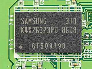
Dynamic random-access memory is a type of random-access semiconductor memory that stores each bit of data in a memory cell, usually consisting of a tiny capacitor and a transistor, both typically based on metal–oxide–semiconductor (MOS) technology. While most DRAM memory cell designs use a capacitor and transistor, some only use two transistors. In the designs where a capacitor is used, the capacitor can either be charged or discharged; these two states are taken to represent the two values of a bit, conventionally called 0 and 1. The electric charge on the capacitors gradually leaks away; without intervention the data on the capacitor would soon be lost. To prevent this, DRAM requires an external memory refresh circuit which periodically rewrites the data in the capacitors, restoring them to their original charge. This refresh process is the defining characteristic of dynamic random-access memory, in contrast to static random-access memory (SRAM) which does not require data to be refreshed. Unlike flash memory, DRAM is volatile memory, since it loses its data quickly when power is removed. However, DRAM does exhibit limited data remanence.

<span class="mw-page-title-main">Synchronous dynamic random-access memory</span> Type of computer memory

Synchronous dynamic random-access memory is any DRAM where the operation of its external pin interface is coordinated by an externally supplied clock signal.

<span class="mw-page-title-main">DIMM</span> Computer memory module

A DIMM, commonly called a RAM stick, comprises a series of dynamic random-access memory integrated circuits. These memory modules are mounted on a printed circuit board and designed for use in personal computers, workstations, printers, and servers. They are the predominant method for adding memory into a computer system. The vast majority of DIMMs are standardized through JEDEC standards, although there are proprietary DIMMs. DIMMs come in a variety of speeds and sizes, but generally are one of two lengths - PC which are 133.35 mm (5.25 in) and laptop (SO-DIMM) which are about half the size at 67.60 mm (2.66 in).

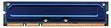
Rambus DRAM (RDRAM), and its successors Concurrent Rambus DRAM (CRDRAM) and Direct Rambus DRAM (DRDRAM), are types of synchronous dynamic random-access memory (SDRAM) developed by Rambus from the 1990s through to the early 2000s. The third-generation of Rambus DRAM, DRDRAM was replaced by XDR DRAM. Rambus DRAM was developed for high-bandwidth applications and was positioned by Rambus as replacement for various types of contemporary memories, such as SDRAM.

The Serial Peripheral Interface (SPI) is a synchronous serial communication interface specification used for short-distance communication, primarily in embedded systems. The interface was developed by Motorola in the mid-1980s and has become a de facto standard. Typical applications include Secure Digital cards and liquid crystal displays.

Rambus Incorporated, founded in 1990, is an American technology company that designs, develops and licenses chip interface technologies and architectures that are used in digital electronics products. The company is well known for inventing RDRAM and for its intellectual property-based litigation following the introduction of DDR-SDRAM memory.

<span class="mw-page-title-main">Double data rate</span>

In computing, a computer bus operating with double data rate (DDR) transfers data on both the rising and falling edges of the clock signal. This is also known as double pumped, dual-pumped, and double transition. The term toggle mode is used in the context of NAND flash memory.

Semiconductor memory is a digital electronic semiconductor device used for digital data storage, such as computer memory. It typically refers to devices in which data is stored within metal–oxide–semiconductor (MOS) memory cells on a silicon integrated circuit memory chip. There are numerous different types using different semiconductor technologies. The two main types of random-access memory (RAM) are static RAM (SRAM), which uses several transistors per memory cell, and dynamic RAM (DRAM), which uses a transistor and a MOS capacitor per cell. Non-volatile memory uses floating-gate memory cells, which consist of a single floating-gate transistor per cell.

Column Address Strobe (CAS) latency, or CL, is the delay in clock cycles between the READ command and the moment data is available. In asynchronous DRAM, the interval is specified in nanoseconds. In synchronous DRAM, the interval is specified in clock cycles. Because the latency is dependent upon a number of clock ticks instead of absolute time, the actual time for an SDRAM module to respond to a CAS event might vary between uses of the same module if the clock rate differs.

XDR2 DRAM was a proposed type of dynamic random-access memory that was offered by Rambus. It was announced on July 7, 2005 and the specification for which was released on March 26, 2008. Rambus has designed XDR2 as an evolution of, and the successor to, XDR DRAM.

Memory refresh is the process of periodically reading information from an area of computer memory and immediately rewriting the read information to the same area without modification, for the purpose of preserving the information. Memory refresh is a background maintenance process required during the operation of semiconductor dynamic random-access memory (DRAM), the most widely used type of computer memory, and in fact is the defining characteristic of this class of memory.

<span class="mw-page-title-main">Fully Buffered DIMM</span>

Fully Buffered DIMM is a memory technology that can be used to increase reliability and density of memory systems. Unlike the parallel bus architecture of traditional DRAMs, an FB-DIMM has a serial interface between the memory controller and the advanced memory buffer (AMB). Conventionally, data lines from the memory controller have to be connected to data lines in every DRAM module, i.e. via multidrop buses. As the memory width increases together with the access speed, the signal degrades at the interface between the bus and the device. This limits the speed and memory density, so FB-DIMMs take a different approach to solve the problem.

GDDR4 SDRAM, an abbreviation for Graphics Double Data Rate 4 Synchronous Dynamic Random-Access Memory, is a type of graphics card memory (SGRAM) specified by the JEDEC Semiconductor Memory Standard. It is a rival medium to Rambus's XDR DRAM. GDDR4 is based on DDR3 SDRAM technology and was intended to replace the DDR2-based GDDR3, but it ended up being replaced by GDDR5 within a year.

Double Data Rate 4 Synchronous Dynamic Random-Access Memory is a type of synchronous dynamic random-access memory with a high bandwidth interface.

<span class="mw-page-title-main">LPDDR</span> Computer hardware

Low-Power Double Data Rate (LPDDR), also known as LPDDR SDRAM, is a type of synchronous dynamic random-access memory that consumes less power and is targeted for mobile computers and devices such as mobile phones. Older variants are also known as Mobile DDR, and abbreviated as mDDR.

<span class="mw-page-title-main">GDDR3 SDRAM</span> Type of graphics card memory

GDDR3 SDRAM is a type of DDR SDRAM specialized for graphics processing units (GPUs) offering less access latency and greater device bandwidths. Its specification was developed by ATI Technologies in collaboration with DRAM vendors including Elpida Memory, Hynix Semiconductor, Infineon and Micron. It was later adopted as a JEDEC standard.

<span class="mw-page-title-main">DDR5 SDRAM</span> Fifth generation of double-data-rate synchronous dynamic random-access memory

Double Data Rate 5 Synchronous Dynamic Random-Access Memory is a type of synchronous dynamic random-access memory. Compared to its predecessor DDR4 SDRAM, DDR5 was planned to reduce power consumption, while doubling bandwidth. The standard, originally targeted for 2018, was released on July 14, 2020.

References