GDDR5 SDRAM

Last updated
GDDR5 SDRAM
Graphics Double Data Rate 5 Synchronous Dynamic Random-Access Memory
Type of RAM
GDDR5 980Ti.jpg
GDDR5 chips on a Nvidia GeForce GTX 980 Ti
Developer JEDEC
Type Synchronous dynamic random-access memory
Generation5th generation
Predecessor GDDR4 SDRAM
Successor GDDR6 SDRAM

Graphics Double Data Rate 5 Synchronous Dynamic Random-Access Memory (GDDR5 SDRAM) is a type of synchronous graphics random-access memory (SGRAM) with a high bandwidth ("double data rate") interface designed for use in graphics cards, game consoles, and high-performance computing. [1] It is a type of GDDR SDRAM (graphics DDR SDRAM).

Contents

Overview

Like its predecessor, GDDR4, GDDR5 is based on DDR3 SDRAM memory, which has double the data lines compared to DDR2 SDRAM. GDDR5 also uses 8-bit wide prefetch buffers similar to GDDR4 and DDR3 SDRAM.

GDDR5 SGRAM conforms to the standards which were set out in the GDDR5 specification by the JEDEC. SGRAM is single-ported. However, it can open two memory pages at once, which simulates the dual-port nature of other VRAM technologies. It uses an 8N-prefetch architecture and DDR interface to achieve high performance operation and can be configured to operate in ×32 mode or ×16 (clamshell) mode which is detected during device initialization. The GDDR5 interface transfers two 32-bit wide data words per write clock (WCK) cycle to/from the I/O pins. Corresponding to the 8N-prefetch, a single write or read access consists of a 256-bit wide two CK clock cycle data transfer at the internal memory core and eight corresponding 32-bit wide one-half WCK clock cycle data transfers at the I/O pins.

GDDR5 operates with two different clock types. A differential command clock (CK) as a reference for address and command inputs, and a forwarded differential write clock (WCK) as a reference for data reads and writes, that runs at twice the CK frequency. Being more precise, the GDDR5 SGRAM uses a total of three clocks: two write clocks associated with two bytes (WCK01 and WCK23) and a single command clock (CK). Taking a GDDR5 with 5  Gbit/s data rate per pin as an example, the CK runs with 1.25 GHz and both WCK clocks at 2.5 GHz. The CK and WCKs are phase aligned during the initialization and training sequence. This alignment allows read and write access with minimum latency.

A single 32-bit GDDR5 chip has about 67 signal pins and the rest are power and grounds in the 170 BGA package.

Commercialization of GDDR5

GDDR5 was revealed by Samsung Electronics in July 2007. They announced that they would mass-produce GDDR5 starting in January 2008. [2]

Hynix Semiconductor introduced the industry's first 60 nm class "1 Gb" (10243 bit) GDDR5 memory in 2007. [3] It supported a bandwidth of 20 GB/s on a 32-bit bus, which enables memory configurations of 1 GB at 160 GB/s with only 8 circuits on a 256-bit bus. The following year, in 2008, Hynix bested this technology with its 50 nm class "1 Gb" GDDR5 memory.

In November 2007, Qimonda, a spin-off of Infineon, demonstrated and sampled GDDR5, [4] and released a paper about the technologies behind GDDR5. [5] As of May 10, 2008, Qimonda announced volume production of 512  Mb GDDR5 components rated at 3.6  Gbit/s (900  MHz), 4.0 Gbit/s (1 GHz), and 4.5 Gbit/s (1.125 GHz). [6]

On November 20, 2009, Elpida Memory announced the opening of the company's Munich Design Center, responsible for Graphics DRAM (GDDR) design and engineering. Elpida received GDDR design assets from Qimonda AG in August 2009 after Qimonda's bankruptcy. The design center has approximately 50 employees and is equipped with high-speed memory testing equipment for use in the design, development and evaluation of Graphics memory. [7] [8] On July 31, 2013, Elpida became a fully owned subsidiary of Micron Technology and based on current public LinkedIn professional profiles, Micron continues to operate the Graphics Design Center in Munich. [9] [10]

Hynix 40 nm class "2 Gb" (2 × 10243 bit) GDDR5 was released in 2010. It operates at 7 GHz effective clock-speed and processes up to 28 GB/s. [11] [12] "2 Gb" GDDR5 memory chips will enable graphics cards with 2 GB or more of onboard memory with 224 GB/s or higher peak bandwidth. On June 25, 2008, AMD became the first company to ship products using GDDR5 memory with its Radeon HD 4870 video card series, incorporating Qimonda's 512 Mb memory modules at 3.6 Gbit/s bandwidth. [13] [14]

In June 2010, Elpida Memory announced the company's 2 Gb GDDR5 memory solution, which was developed at the company's Munich Design Center. The new chip can work at up to 7 GHz effective clock-speed and will be used in graphics cards and other high bandwidth memory applications. [15]

"4 Gb" (4 × 10243 bit) GDDR5 components became available in the third quarter of 2013. Initially released by Hynix, Micron Technology quickly followed up with their implementation releasing in 2014. On February 20, 2013, it was announced that the PlayStation 4 would use sixteen 4 Gb GDDR5 memory chips for a total of 8  GB of GDDR5 @ 176 Gbit/s (CK 1.375 GHz and WCK 2.75 GHz) as combined system and graphics RAM for use with its AMD-powered system on a chip comprising 8 Jaguar cores, 1152 GCN shader processors and AMD TrueAudio. [16] Product teardowns later confirmed the implementation of 4 Gb based GDDR5 memory in the PlayStation 4. [17] [18]

In February 2014, as a result of its acquisition of Elpida, Micron Technology added 2 Gb and 4 Gb GDDR5 products into the company's portfolio of graphics memory solutions. [19]

As of January 15, 2015, Samsung announced in a press release that it had begun mass production of "8 Gb" (8 × 10243 bits) GDDR5 memory chips based on a 20 nm fabrication process. To meet the demand of higher resolution displays (such as 4K) becoming more mainstream, higher density chips are required in order to facilitate larger frame buffers for graphically intensive computation, namely PC gaming and other 3D rendering. Increased bandwidth of the new high-density modules equates to 8 Gbit/s per pin × 170 pins on the BGA package x 32-bits per I/O cycle, or 256 Gbit/s effective bandwidth per chip. [20]

On January 6, 2015, Micron Technology President Mark Adams announced the successful sampling of 8 Gb GDDR5 on the company's fiscal Q1-2015 earnings call. [21] [22] The company then announced, on January 25, 2015, that it had begun commercial shipments of GDDR5 using a 20 nm process technology. [23] [24] [25] The formal announcement of Micron's 8 Gb GDDR5 appeared in the form of a blog post by Kristopher Kido on the company's website September 1, 2015. [26] [27]

GDDR5X

In January 2016, JEDEC standardized GDDR5X SGRAM. [28] GDDR5X targets a transfer rate of 10 to 14 Gbit/s per pin, twice that of GDDR5. [29] Essentially, it provides the memory controller the option to use either a double data rate mode that has a prefetch of 8n, or a quad data rate mode that has a prefetch of 16n. [30] GDDR5 only has a double data rate mode that has an 8n prefetch. [31] GDDR5X also uses 190 pins per chip (190 BGA). [30] By comparison, standard GDDR5 has 170 pins per chip; (170 BGA). [31] It therefore requires a modified PCB. QDR (quad data rate) may be used in reference to the write command clock (WCK) and ODR (Octal Data Rate) in reference to the command clock (CK). [32]

GDDR5X commercialization

GDDR5X on the 1080 Ti GDDR5X 1080ti.jpg
GDDR5X on the 1080 Ti

Micron Technology began sampling GDDR5X chips in March 2016, [33] and began mass production in May 2016. [34]

Nvidia officially announced the first graphics card using GDDR5X, the Pascal-based GeForce GTX 1080 on May 6, 2016. [35] Later, the second graphics card to use GDDR5X, the Nvidia Titan X on July 21, 2016, [36] the GeForce GTX 1080 Ti on February 28, 2017, [37] and Nvidia Titan Xp on April 6, 2017. [38]

See also

Related Research Articles

<span class="mw-page-title-main">DDR SDRAM</span> Type of computer memory

Double Data Rate Synchronous Dynamic Random-Access Memory is a double data rate (DDR) synchronous dynamic random-access memory (SDRAM) class of memory integrated circuits used in computers. DDR SDRAM, also retroactively called DDR1 SDRAM, has been superseded by DDR2 SDRAM, DDR3 SDRAM, DDR4 SDRAM and DDR5 SDRAM. None of its successors are forward or backward compatible with DDR1 SDRAM, meaning DDR2, DDR3, DDR4 and DDR5 memory modules will not work on DDR1-equipped motherboards, and vice versa.

<span class="mw-page-title-main">Synchronous dynamic random-access memory</span> Type of computer memory

Synchronous dynamic random-access memory is any DRAM where the operation of its external pin interface is coordinated by an externally supplied clock signal.

<span class="mw-page-title-main">DDR2 SDRAM</span> Second generation of double-data-rate synchronous dynamic random-access memory

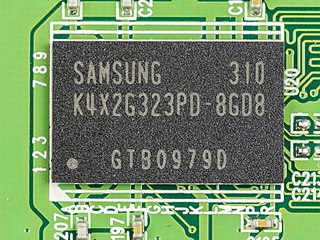
Double Data Rate 2 Synchronous Dynamic Random-Access Memory is a double data rate (DDR) synchronous dynamic random-access memory (SDRAM) interface. It is a JEDEC standard (JESD79-2); first published in September 2003. DDR2 succeeded the original DDR SDRAM specification, and was itself succeeded by DDR3 SDRAM in 2007. DDR2 DIMMs are neither forward compatible with DDR3 nor backward compatible with DDR.

Rambus Inc. is an American technology company that designs, develops and licenses chip interface technologies and architectures that are used in digital electronics products. The company, founded in 1990, is well known for inventing RDRAM and for its intellectual property-based litigation following the introduction of DDR-SDRAM memory.

<span class="mw-page-title-main">Double data rate</span> Method of computer bus operation

In computing, double data rate (DDR) describes a computer bus that transfers data on both the rising and falling edges of the clock signal and hence doubles the memory bandwidth by transferring data twice per clock cycle. This is also known as double pumped, dual-pumped, and double transition. The term toggle mode is used in the context of NAND flash memory.

Double Data Rate 3 Synchronous Dynamic Random-Access Memory is a type of synchronous dynamic random-access memory (SDRAM) with a high bandwidth interface, and has been in use since 2007. It is the higher-speed successor to DDR and DDR2 and predecessor to DDR4 synchronous dynamic random-access memory (SDRAM) chips. DDR3 SDRAM is neither forward nor backward compatible with any earlier type of random-access memory (RAM) because of different signaling voltages, timings, and other factors.

<span class="mw-page-title-main">ATI Rage</span> Series of video cards

The ATI Rage is a series of graphics chipsets developed by ATI Technologies offering graphical user interface (GUI) 2D acceleration, video acceleration, and 3D acceleration developed by ATI Technologies. It is the successor to the ATI Mach series of 2D accelerators.

The G400 is a video card made by Matrox, released in September 1999. The graphics processor contains a 2D GUI, video, and Direct3D 6.0 3D accelerator. Codenamed "Toucan", it was a more powerful and refined version of its predecessor, the G200.

GDDR4 SDRAM, an abbreviation for Graphics Double Data Rate 4 Synchronous Dynamic Random-Access Memory, is a type of graphics card memory (SGRAM) specified by the JEDEC Semiconductor Memory Standard. It is a rival medium to Rambus's XDR DRAM. GDDR4 is based on DDR3 SDRAM technology and was intended to replace the DDR2-based GDDR3, but it ended up being replaced by GDDR5 within a year.

Graphics DDR SDRAM is a type of synchronous dynamic random-access memory (SDRAM) specifically designed for applications requiring high bandwidth, e.g. graphics processing units (GPUs). GDDR SDRAM is distinct from the more widely known types of DDR SDRAM, such as DDR4 and DDR5, although they share some of the same features—including double data rate (DDR) data transfers. As of 2023, GDDR SDRAM has been succeeded by GDDR2, GDDR3, GDDR4, GDDR5, GDDR5X, GDDR6, GDDR6X and GDDR6W.

Double Data Rate 4 Synchronous Dynamic Random-Access Memory is a type of synchronous dynamic random-access memory with a high bandwidth interface.

<span class="mw-page-title-main">LPDDR</span> Computer hardware

Low-Power Double Data Rate (LPDDR), also known as LPDDR SDRAM, is a type of synchronous dynamic random-access memory that consumes less power and is targeted for mobile computers and devices such as mobile phones. Older variants are also known as Mobile DDR, and abbreviated as mDDR.

<span class="mw-page-title-main">GDDR3 SDRAM</span> Type of graphics card memory

GDDR3 SDRAM is a type of DDR SDRAM specialized for graphics processing units (GPUs) offering less access latency and greater device bandwidths. Its specification was developed by ATI Technologies in collaboration with DRAM vendors including Elpida Memory, Hynix Semiconductor, Infineon and Micron. It was later adopted as a JEDEC standard.

Hybrid Memory Cube (HMC) is a high-performance computer random-access memory (RAM) interface for through-silicon via (TSV)-based stacked DRAM memory. HMC competes with the incompatible rival interface High Bandwidth Memory (HBM).

<span class="mw-page-title-main">Pascal (microarchitecture)</span> GPU microarchitecture by Nvidia

Pascal is the codename for a GPU microarchitecture developed by Nvidia, as the successor to the Maxwell architecture. The architecture was first introduced in April 2016 with the release of the Tesla P100 (GP100) on April 5, 2016, and is primarily used in the GeForce 10 series, starting with the GeForce GTX 1080 and GTX 1070, which were released on May 17, 2016, and June 10, 2016, respectively. Pascal was manufactured using TSMC's 16 nm FinFET process, and later Samsung's 14 nm FinFET process.

<span class="mw-page-title-main">DDR5 SDRAM</span> Fifth generation of double-data-rate synchronous dynamic random-access memory

Double Data Rate 5 Synchronous Dynamic Random-Access Memory is the latest type of synchronous dynamic random-access memory. Compared to its predecessor DDR4 SDRAM, DDR5 was planned to reduce power consumption, while doubling bandwidth. The standard, originally targeted for 2018, was released on July 14, 2020.

<span class="mw-page-title-main">High Bandwidth Memory</span> Type of memory used on processors that require high transfer rate memory

High Bandwidth Memory (HBM) is a computer memory interface for 3D-stacked synchronous dynamic random-access memory (SDRAM) initially from Samsung, AMD and SK Hynix. It is used in conjunction with high-performance graphics accelerators, network devices, high-performance datacenter AI ASICs, as on-package cache in CPUs and on-package RAM in upcoming CPUs, and FPGAs and in some supercomputers. The first HBM memory chip was produced by SK Hynix in 2013, and the first devices to use HBM were the AMD Fiji GPUs in 2015.

Graphics Double Data Rate 6 Synchronous Dynamic Random-Access Memory is a type of synchronous graphics random-access memory (SGRAM) with a high bandwidth, "double data rate" interface, designed for use in graphics cards, game consoles, and high-performance computing. It is a type of GDDR SDRAM, and is the successor to GDDR5. Just like GDDR5X it uses QDR in reference to the write command clock (WCK) and ODR in reference to the command clock (CK).

Graphics Double Data Rate 7 Synchronous Dynamic Random-Access Memory is a type of synchronous graphics random-access memory (SGRAM) specified by the JEDEC Semiconductor Memory Standard, with a high bandwidth, "double data rate" interface, designed for use in graphics cards, game consoles, and high-performance computing. It is a type of GDDR SDRAM, and is the successor to GDDR6.

References

  1. Micron TN-ED-01: GDDR5 SGRAM Introduction. Accessed April 11, 2014
  2. Pancescu, Alexandru (July 18, 2007). "Samsung Pushes The GDDR5 Standard Forward". Softpedia . Retrieved 18 September 2019.
  3. "History: 2000s". SK Hynix . Retrieved 8 July 2019.
  4. Register report Archived 2008-07-06 at the Wayback Machine . Retrieved November 2, 2007.
  5. Qimonda GDDR5 Archived 2016-08-26 at the Wayback Machine White Paper
  6. GDDR5 in Production, New Round of Graphics Cards War Imminent., retrieved May 11, 2008
  7. Topalov, Milan. "Elpida officially opens Munich Design Center". www.fabtech.org. Retrieved 2015-09-09.
  8. "Elpida Opens High Speed DRAM Test Laboratory at Munich Design Center | Business Wire". www.businesswire.com. Retrieved 2015-09-09.
  9. "Micron (MU) Completes Elpida Memory, Rexchip Purchases" . Retrieved 2015-09-09.
  10. "Markus Balb | LinkedIn".
  11. Hynix 1H '11 Product Catalog, page 8. Archived 2014-03-13 at the Wayback Machine Accessed July 24, 2014.
  12. Hynix H5GQ2H24AFR Product Overview. Archived 2014-07-23 at the Wayback Machine Accessed July 24, 2014.
  13. Qimonda Press Release. May 21, 2008 Archived September 16, 2008, at the Wayback Machine
  14. AMD Press Release. June 25, 2008
  15. Pop, Sebastian. "Elpida Starts Making GDDR5 Graphics Memory, Delivers 2Gb Chip" . Retrieved 2015-09-09.
  16. "Interview with PS4 system architect". 2013-04-01.
  17. "PlayStation 4 Teardown" . Retrieved 2015-09-09.
  18. teardown.com. "Sony PlayStation 4 Teardown : Board & Chip Shots and Images (Digital Home Teardown)". www.techinsights.com. Archived from the original on 2015-10-02. Retrieved 2015-09-09.
  19. "Micron Technology, Inc.—GDDR5 | DRAM". www.micron.com. Archived from the original on 2016-03-20. Retrieved 2016-09-06.
  20. "Samsung Electronics Starts Mass Producing Industry's First 8-Gigabit Graphics DRAM (GDDR5)". 2015-01-15.
  21. "Micron Technology's (MU) CEO Mark Durcan on Q1 2015 Results—Earnings Call Transcript". Seeking Alpha. Retrieved 2015-09-09.
  22. "Micron: We are sampling 8Gb GDDR5 for 8GB graphics cards" . Retrieved 2015-09-09.
  23. "Micron Technology's (MU) CEO Mark Durcan on Q3 2015 Results—Earnings Call Transcript". Seeking Alpha. Retrieved 2015-09-09.
  24. "Micron begins commercial shipments of 20nm GDDR5 chips" . Retrieved 2015-09-09.
  25. "Micron delivers GDDR5 memory on 20 nm". www.hitechreview.com. Retrieved 2015-09-09.
  26. "Micron Starts Shipping 8Gb GDDR5 Memory For Next Generation Graphics Cards | HotHardware" . Retrieved 2015-09-09.
  27. "Micron Technology, Inc.—Next-Gen Graphics Products Get Extreme Speed From Latest Graphics Memory Solutions". www.micron.com. Retrieved 2015-09-09.
  28. "JEDEC Announces Publication of GDDR5X Graphics Memory Standard". JEDEC. 2016-01-26. Retrieved 2016-02-10.
  29. "JEDEC Publishes GDDR5X Specifications – Double the Bandwidth of GDDR5 With Lowered Power Consumption" . Retrieved 6 June 2016.
  30. 1 2 "GDDR5X SGRAM: MT58K256M32 – 16 Meg x 32 I/O x 16 banks, 32 Meg x 16 I/O x 16 banks" (PDF). Micron Technology. May 2016. Archived from the original (PDF) on February 7, 2017. Retrieved May 29, 2016.
  31. 1 2 "GDDR5 SGRAM: MT51J256M32 – 16 Meg x 32 I/O x 16 banks, 32 Meg x 16 I/O x 16 banks" (PDF). Micron Technology. November 2015. Archived from the original (PDF) on February 7, 2017. Retrieved May 29, 2016.
  32. Smith, Ryan. "Micron Spills on GDDR6X: PAM4 Signaling For Higher Rates, Coming to NVIDIA's RTX 3090". www.anandtech.com.
  33. Shilov, Anton (March 29, 2016). "Micron Begins to Sample GDDR5X Memory, Unveils Specs of Chips". AnandTech . Retrieved 16 July 2019.
  34. Shilov, Anton (May 12, 2016). "Micron Confirms Mass Production of GDDR5X Memory". AnandTech . Retrieved 16 July 2019.
  35. Newsroom, NVIDIA. "A Quantum Leap in Gaming: NVIDIA Introduces GeForce GTX 1080". NVIDIA Newsroom Newsroom.
  36. "The New NVIDIA TITAN X: The Ultimate. Period. - The Official NVIDIA Blog". nvidia.com. 21 July 2016.
  37. Newsroom, NVIDIA. "NVIDIA Introduces the Beastly GeForce GTX 1080 Ti -- Fastest Gaming GPU Ever". NVIDIA Newsroom Newsroom.
  38. "The New Titan Is Here: NVIDIA TITAN Xp - NVIDIA Blog". nvidia.com. 6 April 2017.