Related Research Articles
The GeForce 3 series (NV20) is the third generation of Nvidia's GeForce graphics processing units (GPUs). Introduced in February 2001, it advanced the GeForce architecture by adding programmable pixel and vertex shaders, multisample anti-aliasing and improved the overall efficiency of the rendering process.
The R420 GPU, developed by ATI Technologies, was the company's basis for its 3rd-generation DirectX 9.0/OpenGL 2.0-capable graphics cards. Used first on the Radeon X800, the R420 was produced on a 0.13 micrometer low-K photolithography process and used GDDR-3 memory. The chip was designed for AGP graphics cards.

In computer graphics, a shader is a computer program that calculates the appropriate levels of light, darkness, and color during the rendering of a 3D scene—a process known as shading. Shaders have evolved to perform a variety of specialized functions in computer graphics special effects and video post-processing, as well as general-purpose computing on graphics processing units.
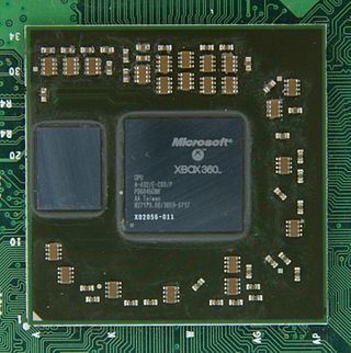
The Xenos is a custom graphics processing unit (GPU) designed by ATI, used in the Xbox 360 video game console developed and produced for Microsoft. Developed under the codename "C1", it is in many ways related to the R520 architecture and therefore very similar to an ATI Radeon X1800 XT series of PC graphics cards as far as features and performance are concerned. However, the Xenos introduced new design ideas that were later adopted in the TeraScale microarchitecture, such as the unified shader architecture. The package contains two separate dies, the GPU and an eDRAM, featuring a total of 337 million transistors.
The R520 is a graphics processing unit (GPU) developed by ATI Technologies and produced by TSMC. It was the first GPU produced using a 90 nm photolithography process.

The R300 GPU, introduced in August 2002 and developed by ATI Technologies, is its third generation of GPU used in Radeon graphics cards. This GPU features 3D acceleration based upon Direct3D 9.0 and OpenGL 2.0, a major improvement in features and performance compared to the preceding R200 design. R300 was the first fully Direct3D 9-capable consumer graphics chip. The processors also include 2D GUI acceleration, video acceleration, and multiple display outputs.

The Radeon R100 is the first generation of Radeon graphics chips from ATI Technologies. The line features 3D acceleration based upon Direct3D 7.0 and OpenGL 1.3, and all but the entry-level versions offloading host geometry calculations to a hardware transform and lighting (T&L) engine, a major improvement in features and performance compared to the preceding Rage design. The processors also include 2D GUI acceleration, video acceleration, and multiple display outputs. "R100" refers to the development codename of the initially released GPU of the generation. It is the basis for a variety of other succeeding products.
In computer graphics, the render output unit (ROP) or raster operations pipeline is a hardware component in modern graphics processing units (GPUs) and one of the final steps in the rendering process of modern graphics cards. The pixel pipelines take pixel and texel information and process it, via specific matrix and vector operations, into a final pixel or depth value; this process is called rasterization. Thus, ROPs control antialiasing, when more than one sample is merged into one pixel. The ROPs perform the transactions between the relevant buffers in the local memory – this includes writing or reading values, as well as blending them together. Dedicated antialiasing hardware used to perform hardware-based antialiasing methods like MSAA is contained in ROPs.
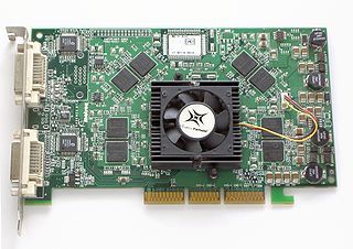
The Matrox Parhelia-512 is a graphics processing unit (GPU) released by Matrox in 2002. It has full support for DirectX 8.1 and incorporates several DirectX 9.0 features. At the time of its release, it was best known for its ability to drive three monitors and its Coral Reef tech demo.
In computer graphics, a video card's pixel fillrate refers to the number of pixels that can be rendered on the screen and written to video memory in one second. Pixel fillrates are given in megapixels per second or in gigapixels per second, and are obtained by multiplying the number of render output units (ROPs) by the clock frequency of the graphics processing unit (GPU) of a video card.
ARB assembly language is a low-level shading language, which can be characterized as an assembly language. It was created by the OpenGL Architecture Review Board (ARB) to standardize GPU instructions controlling the hardware graphics pipeline.
The Radeon HD 8000 series is a family of computer GPUs developed by AMD. AMD was initially rumored to release the family in the second quarter of 2013, with the cards manufactured on a 28 nm process and making use of the improved Graphics Core Next architecture. However the 8000 series turned out to be an OEM rebadge of the 7000 series.
Radeon X800 is a series of graphics cards designed by ATI Technologies Inc. introduced in May of 2004.
The Radeon X700 (RV410) series replaced the X600 in September 2004. X700 Pro is clocked at 425 MHz core, and produced on a 0.11 micrometre process. RV410 used a layout consisting of 8 pixel pipelines connected to 4 ROPs while maintaining the 6 vertex shaders of X800. The 110 nm process was a cost-cutting process, designed not for high clock speeds but for reducing die size while maintaining high yields. An X700 XT was planned for production, and reviewed by various hardware web sites, but was never released. It was believed that X700 XT set too high of a clock ceiling for ATI to profitably produce. X700 XT was also not adequately competitive with nVidia's impressive GeForce 6600GT. ATI would go on produce a card in the X800 series to compete instead.

The R300 GPU, introduced in August 2002 and developed by ATI Technologies, is its third generation of GPU used in Radeon graphics cards. This GPU features 3D acceleration based upon Direct3D 9.0 and OpenGL 2.0, a major improvement in features and performance compared to the preceding R200 design. R300 was the first fully Direct3D 9-capable consumer graphics chip. The processors also include 2D GUI acceleration, video acceleration, and multiple display outputs.
The R200 is the second generation of GPUs used in Radeon graphics cards and developed by ATI Technologies. This GPU features 3D acceleration based upon Microsoft Direct3D 8.1 and OpenGL 1.3, a major improvement in features and performance compared to the preceding Radeon R100 design. The GPU also includes 2D GUI acceleration, video acceleration, and multiple display outputs. "R200" refers to the development codename of the initially released GPU of the generation. It is the basis for a variety of other succeeding products.
TeraScale is the codename for a family of graphics processing unit microarchitectures developed by ATI Technologies/AMD and their second microarchitecture implementing the unified shader model following Xenos. TeraScale replaced the old fixed-pipeline microarchitectures and competed directly with Nvidia's first unified shader microarchitecture named Tesla.
This is a glossary of terms relating to computer graphics.
References
- ↑ "Dev Hardware - The Graphics Pipeline". Archived from the original on 2006-05-28. Retrieved 11 May 2006.