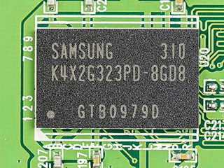
Stored information
For a memory module to support SPD, the JEDEC standards require that certain parameters be in the lower 128 bytes of an EEPROM located on the memory module. These bytes contain timing parameters, manufacturer, serial number and other useful information about the module. Devices utilizing the memory automatically determine key parameters of the module by reading this information. For example, the SPD data on an SDRAM module might provide information about the CAS latency so the system can set this correctly without user intervention.
The SPD EEPROM firmware is accessed using SMBus, a variant of the I2C protocol. This reduces the number of communication pins on the module to just two: a clock signal and a data signal. The EEPROM shares ground pins with the RAM, has its own power pin, and has three additional pins (SA0–2) to identify the slot, which are used to assign the EEPROM a unique address in the range 0x50–0x57. Not only can the communication lines be shared among 8 memory modules, the same SMBus is commonly used on motherboards for system health monitoring tasks such as reading power supply voltages, CPU temperatures, and fan speeds.
SPD EEPROMs also respond to I2C addresses 0x30–0x37 if they have not been write protected, and an extension (TSE series) uses addresses 0x18–0x1F to access an optional on-chip temperature sensor. All those values are seven-bit I2C addresses formed by a Device Type Identifier Code prefix (DTIC) with SA0-2: to read (1100) from slot 3, one uses 110 0011 = 0x33. With a final R/W bit it forms the 8-bit Device Select Code. [2] Note that the semantics of slot-id is different for write-protection operations: for them they can be not passed by the SA pins at all. [3]
Before SPD, memory chips were spotted with parallel presence detect (PPD). PPD used a separate pin for each bit of information, which meant that only the speed and density of the memory module could be stored because of the limited space for pins.
SDR SDRAM

The first SPD specification was issued by JEDEC and tightened up by Intel as part of its PC100 memory specification introduced in 1998. [4] [5] [6] Most values specified are in binary-coded decimal form. The most significant nibble can contain values from 10 to 15, and in some cases extends higher. In such cases, the encodings for 1, 2 and 3 are instead used to encode 16, 17 and 18. A most significant nibble of 0 is reserved to represent "undefined".
The SPD ROM defines up to three DRAM timings, for three CAS latencies specified by set bits in byte 18. First comes the highest CAS latency (fastest clock), then two lower CAS latencies with progressively lower clock speeds.
| Byte | Bit | Notes | ||||||||
|---|---|---|---|---|---|---|---|---|---|---|
| (dec.) | (hex.) | 7 | 6 | 5 | 4 | 3 | 2 | 1 | 0 | |
| 0 | 0x00 | Number of bytes present | Typically 128 | |||||||
| 1 | 0x01 | log2(size of SPD EEPROM) | Typically 8 (256 bytes) | |||||||
| 2 | 0x02 | Basic memory type (4: SPD SDRAM) | ||||||||
| 3 | 0x03 | Bank 2 row address bits (0–15) | Bank 1 row address bits (1–15) | Bank 2 is 0 if same as bank 1 | ||||||
| 4 | 0x04 | Bank 2 column address bits (0–15) | Bank 1 column address bits (1–15) | Bank 2 is 0 if same as bank 1 | ||||||
| 5 | 0x05 | Number of RAM banks on module (1–255) | Commonly 1 or 2 | |||||||
| 6 | 0x06 | Module data width low byte | Commonly 64, or 72 for ECC DIMMs | |||||||
| 7 | 0x07 | Module data width high byte | 0, unless width ≥ 256 bits | |||||||
| 8 | 0x08 | Interface voltage level of this assembly (not the same as Vcc supply voltage) (0–4) | Decoded by table lookup | |||||||
| 9 | 0x09 | Nanoseconds (0–15) | Tenths of nanoseconds (0.0–0.9) | Clock cycle time at highest CAS latency | ||||||
| 10 | 0x0a | Nanoseconds (0–15) | Tenths of nanoseconds (0.0–0.9) | SDRAM access time from clock (tAC) | ||||||
| 11 | 0x0b | DIMM configuration type (0–2): non-ECC, parity, ECC | Table lookup | |||||||
| 12 | 0x0c | Self | Refresh period (0–5): 64, 256, 128, 32, 16, 8 kHz | Refresh requirements | ||||||
| 13 | 0x0d | Bank 2 2× | Bank 1 primary SDRAM width (1–127, usually 8) | Width of bank 1 data SDRAM devices. Bank 2 may be same width, or 2× width if bit 7 is set. | ||||||
| 14 | 0x0e | Bank 2 2× | Bank 1 ECC SDRAM width (0–127) | Width of bank 1 ECC/parity SDRAM devices. Bank 2 may be same width, or 2× width if bit 7 is set. | ||||||
| 15 | 0x0f | Clock delay for random column reads | Typically 1 | |||||||
| 16 | 0x10 | Page | — | — | — | 8 | 4 | 2 | 1 | Burst lengths supported (bitmap) |
| 17 | 0x11 | Banks per SDRAM device (1–255) | Typically 2 or 4 | |||||||
| 18 | 0x12 | — | 7 | 6 | 5 | 4 | 3 | 2 | 1 | CAS latencies supported (bitmap) |
| 19 | 0x13 | — | 6 | 5 | 4 | 3 | 2 | 1 | 0 | CS latencies supported (bitmap) |
| 20 | 0x14 | — | 6 | 5 | 4 | 3 | 2 | 1 | 0 | WE latencies supported (bitmap) |
| 21 | 0x15 | — | Redundant | Diff. clock | Registered data | Buffered data | On-card PLL | Registered addr. | Buffered addr. | Memory module feature bitmap |
| 22 | 0x16 | — | — | Upper Vcc (supply voltage) tolerance | Lower Vcc (supply voltage) tolerance | Write/1 read burst | Precharge all | Auto-precharge | Early RAS precharge | Memory chip feature support bitmap |
| 23 | 0x17 | Nanoseconds (4–18) | Tenths of nanoseconds (0–9: 0.0–0.9) | Clock cycle time at medium CAS latency | ||||||
| 24 | 0x18 | Nanoseconds (4–18) | Tenths of nanoseconds (0–9: 0.0–0.9) | Data access time from clock (tAC) | ||||||
| 25 | 0x19 | Nanoseconds (1–63) | 0.25 ns (0–3: 0.00–0.75) | Clock cycle time at short CAS latency. | ||||||
| 26 | 0x1a | Nanoseconds (1–63) | 0.25 ns (0–3: 0.00–0.75) | Data access time from clock (tAC) | ||||||
| 27 | 0x1b | Nanoseconds (1–255) | Minimum row precharge time (tRP) | |||||||
| 28 | 0x1c | Nanoseconds (1–255) | Minimum row active–row active delay (tRRD) | |||||||
| 29 | 0x1d | Nanoseconds (1–255) | Minimum RAS to CAS delay (tRCD) | |||||||
| 30 | 0x1e | Nanoseconds (1–255) | Minimum active to precharge time (tRAS) | |||||||
| 31 | 0x1f | 512 MiB | 256 MiB | 128 MiB | 64 MiB | 32 MiB | 16 MiB | 8 MiB | 4 MiB | Module bank density (bitmap). Two bits set if different size banks. |
| 32 | 0x20 | Sign (1: −) | Nanoseconds (0–7) | Tenths of nanoseconds (0–9: 0.0–0.9) | Address/command setup time from clock | |||||
| 33 | 0x21 | Sign (1: −) | Nanoseconds (0–7) | Tenths of nanoseconds (0–9: 0.0–0.9) | Address/command hold time after clock | |||||
| 34 | 0x22 | Sign (1: −) | Nanoseconds (0–7) | Tenths of nanoseconds (0–9: 0.0–0.9) | Data input setup time from clock | |||||
| 35 | 0x23 | Sign (1: −) | Nanoseconds (0–7) | Tenths of nanoseconds (0–9: 0.0–0.9) | Data input hold time after clock | |||||
| 36–61 | 0x24–0x3d | Reserved | For future standardization | |||||||
| 62 | 0x3e | Major revision (0–9) | Minor revision (0–9) | SPD revision level; e.g., 1.2 | ||||||
| 63 | 0x3f | Checksum | Sum of bytes 0–62, not then negated | |||||||
| 64–71 | 0x40–47 | Manufacturer JEDEC id. | Stored little-endian, trailing zero-padded | |||||||
| 72 | 0x48 | Module manufacturing location | Vendor-specific code | |||||||
| 73–90 | 0x49–0x5a | Module part number | ASCII, space-padded | |||||||
| 91–92 | 0x5b–0x5c | Module revision code | Vendor-specific code | |||||||
| 93 | 0x5d | Tens of years (0–9: 0–90) | Years (0–9) | Manufacturing date (YYWW) | ||||||
| 94 | 0x5e | Tens of weeks (0–5: 0–50) | Weeks (0–9) | |||||||
| 95–98 | 0x5f–0x62 | Module serial number | Vendor-specific code | |||||||
| 99–125 | 0x63–0x7f | Manufacturer-specific data | Could be enhanced performance profile | |||||||
| 126 | 0x7e | 0x66[ sic ] for 66 MHz, 0x64 for 100 MHz | Intel frequency support | |||||||
| 127 | 0x7f | CLK0 | CLK1 | CLK3 | CLK3 | 90/100 °C | CL3 | CL2 | Concurrent AP | Intel feature bitmap |
DDR SDRAM
The DDR DIMM SPD format is an extension of the SDR SDRAM format. Mostly, parameter ranges are rescaled to accommodate higher speeds.
| Byte | Bit | Notes | ||||||||
|---|---|---|---|---|---|---|---|---|---|---|
| (dec.) | (hex.) | 7 | 6 | 5 | 4 | 3 | 2 | 1 | 0 | |
| 0 | 0x00 | Number of bytes written | Typically 128 | |||||||
| 1 | 0x01 | log2(size of SPD EEPROM) | Typically 8 (256 bytes) | |||||||
| 2 | 0x02 | Basic memory type (7 = DDR SDRAM) | ||||||||
| 3 | 0x03 | Bank 2 row address bits (0–15) | Bank 1 row address bits (1–15) | Bank 2 is 0 if same as bank 1. | ||||||
| 4 | 0x04 | Bank 2 column address bits (0–15) | Bank 1 column address bits (1–15) | Bank 2 is 0 if same as bank 1. | ||||||
| 5 | 0x05 | Number of RAM banks on module (1–255) | Commonly 1 or 2 | |||||||
| 6 | 0x06 | Module data width low byte | Commonly 64, or 72 for ECC DIMMs | |||||||
| 7 | 0x07 | Module data width high byte | 0, unless width ≥ 256 bits | |||||||
| 8 | 0x08 | Interface voltage level of this assembly (not the same as Vcc supply voltage) (0–5) | Decoded by table lookup | |||||||
| 9 | 0x09 | Nanoseconds (0–15) | Tenths of nanoseconds (0.0–0.9) | Clock cycle time at highest CAS latency. | ||||||
| 10 | 0x0a | Tenths of nanoseconds (0.0–0.9) | Hundredths of nanoseconds (0.00–0.09) | SDRAM access time from clock (tAC) | ||||||
| 11 | 0x0b | DIMM configuration type (0–2): non-ECC, parity, ECC | Table lookup | |||||||
| 12 | 0x0c | Self | Refresh period (0–5): 64, 256, 128, 32, 16, 8 kHz | Refresh requirements | ||||||
| 13 | 0x0d | Bank 2 2× | Bank 1 primary SDRAM width (1–127) | Width of bank 1 data SDRAM devices. Bank 2 may be same width, or 2× width if bit 7 is set. | ||||||
| 14 | 0x0e | Bank 2 2× | Bank 1 ECC SDRAM width (0–127) | Width of bank 1 ECC/parity SDRAM devices. Bank 2 may be same width, or 2× width if bit 7 is set. | ||||||
| 15 | 0x0f | Clock delay for random column reads | Typically 1 | |||||||
| 16 | 0x10 | Page | — | — | — | 8 | 4 | 2 | 1 | Burst lengths supported (bitmap) |
| 17 | 0x11 | Banks per SDRAM device (1–255) | Typically 4 | |||||||
| 18 | 0x12 | — | 4 | 3.5 | 3 | 2.5 | 2 | 1.5 | 1 | CAS latencies supported (bitmap) |
| 19 | 0x13 | — | 6 | 5 | 4 | 3 | 2 | 1 | 0 | CS latencies supported (bitmap) |
| 20 | 0x14 | — | 6 | 5 | 4 | 3 | 2 | 1 | 0 | WE latencies supported (bitmap) |
| 21 | 0x15 | — | x | Diff clock | FET switch external enable | FET switch on-board enable | On-card PLL | Registered | Buffered | Memory module feature bitmap |
| 22 | 0x16 | Fast AP | Concurrent auto precharge | Upper Vcc (supply voltage) tolerance | Lower Vcc (supply voltage) tolerance | — | — | — | Includes weak driver | Memory chip feature bitmap |
| 23 | 0x17 | Nanoseconds (0–15) | Tenths of nanoseconds (0.0–0.9) | Clock cycle time at medium CAS latency. | ||||||
| 24 | 0x18 | Tenths of nanoseconds (0.0–0.9) | Hundredths of nanoseconds (0.00–0.09) | Data access time from clock (tAC) | ||||||
| 25 | 0x19 | Nanoseconds (0–15) | Tenths of nanoseconds (0.0–0.9) | Clock cycle time at short CAS latency. | ||||||
| 26 | 0x1a | Tenths of nanoseconds (0.0–0.9) | Hundredths of nanoseconds (0.00–0.09) | Data access time from clock (tAC) | ||||||
| 27 | 0x1b | Nanoseconds (1–63) | 0.25 ns (0–0.75) | Minimum row precharge time (tRP) | ||||||
| 28 | 0x1c | Nanoseconds (1–63) | 0.25 ns (0–0.75) | Minimum row active–row active delay (tRRD) | ||||||
| 29 | 0x1d | Nanoseconds (1–63) | 0.25 ns (0–0.75) | Minimum RAS to CAS delay (tRCD) | ||||||
| 30 | 0x1e | Nanoseconds (1–255) | Minimum active to precharge time (tRAS) | |||||||
| 31 | 0x1f | 512 MiB | 256 MiB | 128 MiB | 64 MiB | 32 MiB | 16 MiB/ 4 GiB | 8 MiB/ 2 GiB | 4 MiB/ 1 GiB | Module bank density (bitmap). Two bits set if different size banks. |
| 32 | 0x20 | Tenths of nanoseconds (0.0–0.9) | Hundredths of nanoseconds (0.00–0.09) | Address/command setup time from clock | ||||||
| 33 | 0x21 | Tenths of nanoseconds (0.0–0.9) | Hundredths of nanoseconds (0.00–0.09) | Address/command hold time after clock | ||||||
| 34 | 0x22 | Tenths of nanoseconds (0.0–0.9) | Hundredths of nanoseconds (0.00–0.09) | Data input setup time from clock | ||||||
| 35 | 0x23 | Tenths of nanoseconds (0.0–0.9) | Hundredths of nanoseconds (0.00–0.09) | Data input hold time after clock | ||||||
| 36–40 | 0x24–0x28 | Reserved | Superset information | |||||||
| 41 | 0x29 | Nanoseconds (1–255) | Minimum active to active/refresh time (tRC) | |||||||
| 42 | 0x2a | Nanoseconds (1–255) | Minimum refresh to active/refresh time (tRFC) | |||||||
| 43 | 0x2b | Nanoseconds (1–63, or 255: no maximum) | 0.25 ns (0–0.75) | Maximum clock cycle time (tCK max.) | ||||||
| 44 | 0x2c | Hundredths of nanoseconds (0.01–2.55) | Maximum skew, DQS to any DQ. (tDQSQ max.) | |||||||
| 45 | 0x2d | Tenths of nanoseconds (0.0–1.2) | Hundredths of nanoseconds (0.00–0.09) | Read data hold skew factor (tQHS) | ||||||
| 46 | 0x2e | Reserved | For future standardization | |||||||
| 47 | 0x2f | — | Height | Height of DIMM module, table lookup | ||||||
| 48–61 | 0x30–0x3d | Reserved | For future standardization | |||||||
| 62 | 0x3e | Major revision (0–9) | Minor revision (0–9) | SPD revision level, 0.0 or 1.0 | ||||||
| 63 | 0x3f | Checksum | Sum of bytes 0–62, not then negated | |||||||
| 64–71 | 0x40–47 | Manufacturer JEDEC id. | Stored little-endian, trailing zero-padded | |||||||
| 72 | 0x48 | Module manufacturing location | Vendor-specific code | |||||||
| 73–90 | 0x49–0x5a | Module part number | ASCII, space-padded | |||||||
| 91–92 | 0x5b–0x5c | Module revision code | Vendor-specific code | |||||||
| 93 | 0x5d | Tens of years (0–90) | Years (0–9) | Manufacturing date (YYWW) | ||||||
| 94 | 0x5e | Tens of weeks (0–50) | Weeks (0–9) | |||||||
| 95–98 | 0x5f–0x62 | Module serial number | Vendor-specific code | |||||||
| 99–127 | 0x63–0x7f | Manufacturer-specific data | Could be enhanced performance profile | |||||||
DDR2 SDRAM
The DDR2 SPD standard makes a number of changes, but is roughly similar to the above. One notable deletion is the confusing and little-used support for DIMMs with two ranks of different sizes.
For cycle time fields (bytes 9, 23, 25 and 49), which are encoded in BCD, some additional encodings are defined for the tenths digit to represent some common timings exactly:
| Hex | Binary | Significance |
|---|---|---|
| A | 1010 | 0.25 (1⁄4) |
| B | 1011 | 0.33 (1⁄3) |
| C | 1100 | 0.66 (2⁄3) |
| D | 1101 | 0.75 (3⁄4) |
| E | 1110 | 0.875 (7⁄8, Nvidia XMP extension) |
| F | 1111 | Reserved |
| Byte | Bit | Notes | ||||||||
|---|---|---|---|---|---|---|---|---|---|---|
| Dec | Hex | 7 | 6 | 5 | 4 | 3 | 2 | 1 | 0 | |
| 0 | 0x00 | Number of bytes written | Typically 128 | |||||||
| 1 | 0x01 | log2(size of SPD EEPROM) | Typically 8 (256 bytes) | |||||||
| 2 | 0x02 | Basic memory type (8 = DDR2 SDRAM) | ||||||||
| 3 | 0x03 | Reserved | Row address bits (1–15) | |||||||
| 4 | 0x04 | Reserved | Column address bits (1–15) | |||||||
| 5 | 0x05 | Vertical height | Stack? | ConC? | Ranks−1 (1–8) | Commonly 0 or 1, meaning 1 or 2 | ||||
| 6 | 0x06 | Module data width | Commonly 64, or 72 for ECC DIMMs | |||||||
| 7 | 0x07 | Reserved | ||||||||
| 8 | 0x08 | Interface voltage level of this assembly (not the same as Vcc supply voltage) (0–5) | Decoded by table lookup. Commonly 5 = SSTL 1.8 V | |||||||
| 9 | 0x09 | Nanoseconds (0–15) | Tenths of nanoseconds (0.0–0.9) | Clock cycle time at highest CAS latency. | ||||||
| 10 | 0x0a | Tenths of nanoseconds (0.0–0.9) | Hundredths of nanoseconds (0.00–0.09) | SDRAM access time from clock (tAC) | ||||||
| 11 | 0x0b | DIMM configuration type (0–2): non-ECC, parity, ECC | Table lookup | |||||||
| 12 | 0x0c | Self | Refresh period (0–5): 64, 256, 128, 32, 16, 8 kHz | Refresh requirements | ||||||
| 13 | 0x0d | Primary SDRAM width (1–255) | Commonly 8 (module built from ×8 parts) or 16 | |||||||
| 14 | 0x0e | ECC SDRAM width (0–255) | Width of bank ECC/parity SDRAM devices. Commonly 0 or 8. | |||||||
| 15 | 0x0f | Reserved | ||||||||
| 16 | 0x10 | — | — | — | — | 8 | 4 | — | — | Burst lengths supported (bitmap) |
| 17 | 0x11 | Banks per SDRAM device (1–255) | Typically 4 or 8 | |||||||
| 18 | 0x12 | 7 | 6 | 5 | 4 | 3 | 2 | — | — | CAS latencies supported (bitmap) |
| 19 | 0x13 | Reserved | ||||||||
| 20 | 0x14 | — | — | Mini-UDIMM | Mini-RDIMM | Micro-DIMM | SO-DIMM | UDIMM | RDIMM | DIMM type of this assembly (bitmap) |
| 21 | 0x15 | — | Module is analysis probe | — | FET switch external enable | — | — | — | — | Memory module feature bitmap |
| 22 | 0x16 | — | — | — | — | — | — | — | Includes weak driver | Memory chip feature bitmap |
| 23 | 0x17 | Nanoseconds (0–15) | Tenths of nanoseconds (0.0–0.9) | Clock cycle time at medium CAS latency. | ||||||
| 24 | 0x18 | Tenths of nanoseconds (0.0–0.9) | Hundredths of nanoseconds (0.00–0.09) | Data access time from clock (tAC) | ||||||
| 25 | 0x19 | Nanoseconds (0–15) | Tenths of nanoseconds (0.0–0.9) | Clock cycle time at short CAS latency. | ||||||
| 26 | 0x1a | Tenths of nanoseconds (0.0–0.9) | Hundredths of nanoseconds (0.00–0.09) | Data access time from clock (tAC) | ||||||
| 27 | 0x1b | Nanoseconds (1–63) | 1/4 ns (0–0.75) | Minimum row precharge time (tRP) | ||||||
| 28 | 0x1c | Nanoseconds (1–63) | 1/4 ns (0–0.75) | Minimum row active–row active delay (tRRD) | ||||||
| 29 | 0x1d | Nanoseconds (1–63) | 1/4 ns (0–0.75) | Minimum RAS to CAS delay (tRCD) | ||||||
| 30 | 0x1e | Nanoseconds (1–255) | Minimum active to precharge time (tRAS) | |||||||
| 31 | 0x1f | 512 MiB | 256 MiB | 128 MiB | 16 GiB | 8 GiB | 4 GiB | 2 GiB | 1 GiB | Size of each rank (bitmap). |
| 32 | 0x20 | Tenths of nanoseconds (0.0–1.2) | Hundredths of nanoseconds (0.00–0.09) | Address/command setup time from clock | ||||||
| 33 | 0x21 | Tenths of nanoseconds (0.0–1.2) | Hundredths of nanoseconds (0.00–0.09) | Address/command hold time after clock | ||||||
| 34 | 0x22 | Tenths of nanoseconds (0.0–0.9) | Hundredths of nanoseconds (0.00–0.09) | Data input setup time from strobe | ||||||
| 35 | 0x23 | Tenths of nanoseconds (0.0–0.9) | Hundredths of nanoseconds (0.00–0.09) | Data input hold time after strobe | ||||||
| 36 | 0x24 | Nanoseconds (1–63) | 0.25 ns (0–0.75) | Minimum write recovery time (tWR) | ||||||
| 37 | 0x25 | Nanoseconds (1–63) | 0.25 ns (0–0.75) | Internal write to read command delay (tWTR) | ||||||
| 38 | 0x26 | Nanoseconds (1–63) | 0.25 ns (0–0.75) | Internal read to precharge command delay (tRTP) | ||||||
| 39 | 0x27 | Reserved | Reserved for "memory analysis probe characteristics" | |||||||
| 40 | 0x28 | — | tRC fractional ns (0–5): 0, 0.25, 0.33, 0.5, 0.66, 0.75 | tRFC fractional ns (0–5): 0, 0.25, 0.33, 0.5, 0.66, 0.75 | tRFC + 256 ns | Extension of bytes 41 and 42. | ||||
| 41 | 0x29 | Nanoseconds (1–255) | Minimum active to active/refresh time (tRC) | |||||||
| 42 | 0x2a | Nanoseconds (1–255) | Minimum refresh to active/refresh time (tRFC) | |||||||
| 43 | 0x2b | Nanoseconds (0–15) | Tenths of nanoseconds (0.0–0.9) | Maximum clock cycle time (tCK max) | ||||||
| 44 | 0x2c | Hundredths of nanoseconds (0.01–2.55) | Maximum skew, DQS to any DQ. (tDQSQ max) | |||||||
| 45 | 0x2d | Hundredths of nanoseconds (0.01–2.55) | Read data hold skew factor (tQHS) | |||||||
| 46 | 0x2e | Microseconds (1–255) | PLL relock time | |||||||
| 47–61 | 0x2f–0x3d | Reserved | For future standardization. | |||||||
| 62 | 0x3e | Major revision (0–9) | Minor revision (0.0–0.9) | SPD revision level, usually 1.0 | ||||||
| 63 | 0x3f | Checksum | Sum of bytes 0–62, not negated | |||||||
| 64–71 | 0x40–47 | Manufacturer JEDEC ID | Stored little-endian, trailing zero-pad | |||||||
| 72 | 0x48 | Module manufacturing location | Vendor-specific code | |||||||
| 73–90 | 0x49–0x5a | Module part number | ASCII, space-padded (limited to (,-,), A–Z, a–z, 0–9, space) | |||||||
| 91–92 | 0x5b–0x5c | Module revision code | Vendor-specific code | |||||||
| 93 | 0x5d | Years since 2000 (0–255) | Manufacturing date (YYWW) | |||||||
| 94 | 0x5e | Weeks (1–52) | ||||||||
| 95–98 | 0x5f–0x62 | Module serial number | Vendor-specific code | |||||||
| 99–127 | 0x63–0x7f | Manufacturer-specific data | Could be enhanced performance profile | |||||||
DDR3 SDRAM
The DDR3 SDRAM standard significantly overhauls and simplifies the SPD contents layout. Instead of a number of BCD-encoded nanosecond fields, some "timebase" units are specified to high precision, and various timing parameters are encoded as multiples of that base unit. [10] Further, the practice of specifying different time values depending on the CAS latency has been dropped; now there are just a single set of timing parameters.
Revision 1.1 lets some parameters be expressed as a "medium time base" value plus a (signed, −128 +127) "fine time base" correction. Generally, the medium time base is 1/8 ns (125 ps), and the fine time base is 1, 2.5 or 5 ps. For compatibility with earlier versions that lack the correction, the medium time base number is usually rounded up and the correction is negative. Values that work this way are:
| MTB byte | FTB byte | Value |
|---|---|---|
| 12 | 34 | tCKmin, minimum clock period |
| 16 | 35 | tAAmin, minimum CAS latency time |
| 18 | 36 | tRCDmin, minimum RAS# to CAS# delay |
| 20 | 37 | tRPmin, minimum row precharge delay |
| 21, 23 | 38 | tRCmin, minimum active to active/precharge delay |
| Byte | Bit | Notes | ||||||||
|---|---|---|---|---|---|---|---|---|---|---|
| Dec | Hex | 7 | 6 | 5 | 4 | 3 | 2 | 1 | 0 | |
| 0 | 0x00 | Exclude serial from CRC | SPD bytes total (undef/256) | SPD bytes used (undef/128/176/256) | ||||||
| 1 | 0x01 | SPD major revision | SPD minor revision | 1.0, 1.1, 1.2 or 1.3 | ||||||
| 2 | 0x02 | Basic memory type (11 = DDR3 SDRAM) | Type of RAM chips | |||||||
| 3 | 0x03 | Reserved | Module type | Type of module; e.g., 2 = Unbuffered DIMM, 3 = SO-DIMM, 11=LRDIMM | ||||||
| 4 | 0x04 | — | Bank address bits−3 | log2(bits per chip)−28 | Zero means 8 banks, 256 Mibit. | |||||
| 5 | 0x05 | — | Row address bits−12 | Column address bits−9 | ||||||
| 6 | 0x06 | Reserved | 1.25 V | 1.35 V | Not 1.5 V | Modules voltages supported. 1.5 V is default. | ||||
| 7 | 0x07 | — | ranks−1 | log2(I/O bits/chip)−2 | Module organization | |||||
| 8 | 0x08 | — | ECC bits (001=8) | log2(data bits)−3 | 0x03 for 64-bit, non-ECC DIMM. | |||||
| 9 | 0x09 | Dividend, picoseconds (1–15) | Divisor, picoseconds (1–15) | Fine Time Base, dividend/divisor | ||||||
| 10 | 0x0a | Dividend, nanoseconds (1–255) | Medium Time Base, dividend/divisor; commonly 1/8 | |||||||
| 11 | 0x0b | Divisor, nanoseconds (1–255) | ||||||||
| 12 | 0x0c | Minimum cycle time tCKmin | In multiples of MTB | |||||||
| 13 | 0x0d | Reserved | ||||||||
| 14 | 0x0e | 11 | 10 | 9 | 8 | 7 | 6 | 5 | 4 | CAS latencies supported (bitmap) |
| 15 | 0x0f | — | 18 | 17 | 16 | 15 | 14 | 13 | 12 | |
| 16 | 0x10 | Minimum CAS latency time, tAAmin | In multiples of MTB; e.g., 80/8 ns. | |||||||
| 17 | 0x11 | Minimum write recovery time, tWRmin | In multiples of MTB; e.g., 120/8 ns. | |||||||
| 18 | 0x12 | Minimum RAS to CAS delay time, tRCDmin | In multiples of MTB; e.g., 100/8 ns. | |||||||
| 19 | 0x13 | Minimum row to row active delay time, tRRDmin | In multiples of MTB; e.g., 60/8 ns. | |||||||
| 20 | 0x14 | Minimum row precharge time, tRPmin | In multiples of MTB; e.g., 100/8 ns. | |||||||
| 21 | 0x15 | tRCmin, bits 11:8 | tRASmin, bits 11:8 | Upper 4 bits of bytes 23 and 22 | ||||||
| 22 | 0x16 | Minimum active to time, tRASmin, bits 7:0 | In multiples of MTB; e.g., 280/8 ns. | |||||||
| 23 | 0x17 | Minimum active to active/refresh, tRCmin, bits 7:0 | In multiples of MTB; e.g., 396/8 ns. | |||||||
| 24 | 0x18 | Minimum refresh recovery delay, tRFCmin, bits 7:0 | In multiples of MTB; e.g., 1280/8 ns. | |||||||
| 25 | 0x19 | Minimum refresh recovery delay, tRFCmin, bits 15:8 | ||||||||
| 26 | 0x1a | Minimum internal write to read delay, tWTRmin | In multiples of MTB; e.g., 60/8 ns. | |||||||
| 27 | 0x1b | Minimum internal read to precharge delay, tRTPmin | In multiples of MTB; e.g., 60/8 ns. | |||||||
| 28 | 0x1c | Reserved | tFAWmin, bits 11:8 | In multiples of MTB; e.g., 240/8 ns. | ||||||
| 29 | 0x1d | Minimum four activate window delay tFAWmin, bits 7:0 | ||||||||
| 30 | 0x1e | DLL-off | — | RZQ/7 | RZQ/6 | SDRAM optional features support bitmap | ||||
| 31 | 0x1f | PASR | — | ODTS | ASR | ETR 1× | ETR (95 °C) | SDRAM thermal and refresh options | ||
| 32 | 0x20 | Present | Accuracy (TBD; currently 0 = undefined) | DIMM thermal sensor present? | ||||||
| 33 | 0x21 | Nonstd. | Die count | — | Signal load | Nonstandard SDRAM device type (e.g., stacked die) | ||||
| 34 | 0x22 | tCKmin correction (new for 1.1) | Signed multiple of FTB, added to byte 12 | |||||||
| 35 | 0x23 | tAAmin correction (new for 1.1) | Signed multiple of FTB, added to byte 16 | |||||||
| 36 | 0x24 | tRCDmin correction (new for 1.1) | Signed multiple of FTB, added to byte 18 | |||||||
| 37 | 0x25 | tRPmin correction (new for 1.1) | Signed multiple of FTB, added to byte 20 | |||||||
| 38 | 0x26 | tRCmin correction (new for 1.1) | Signed multiple of FTB, added to byte 23 | |||||||
| 39–40 | 0x27–0x28 | Reserved | For future standardization. | |||||||
| 41 | 0x29 | Vendor specific | tMAW | Maximum Activate Count (MAC) (untested/700k/600k/.../200k/reserved/∞) | For row hammer mitigation | |||||
| 42–59 | 0x2a–0x3b | Reserved | For future standardization. | |||||||
| 60 | 0x3c | — | Module height, mm (1–31, >45) | Module nominal height | ||||||
| 61 | 0x3d | Back thickness, mm (1–16) | Front thickness, mm (1–16) | Module thickness, value = ceil(mm) − 1 | ||||||
| 62 | 0x3e | Design | Revision | JEDEC design number | JEDEC reference design used (11111=none) | |||||
| 63–116 | 0x3f–0x74 | Module-specific section | Differs between registered/unbuffered | |||||||
| 117 | 0x75 | Module manufacturer ID, lsbyte | Assigned by JEP-106 | |||||||
| 118 | 0x76 | Module manufacturer ID, msbyte | ||||||||
| 119 | 0x77 | Module manufacturing location | Vendor-specific code | |||||||
| 120 | 0x78 | Tens of years | Years | Manufacturing year (BCD) | ||||||
| 121 | 0x79 | Tens of weeks | Weeks | Manufacturing week (BCD) | ||||||
| 122–125 | 0x7a–0x7d | Module serial number | Vendor-specific code | |||||||
| 126–127 | 0x7e–0x7f | SPD CRC-16 | Includes bytes 0–116 or 0–125; see byte 0 bit 7 | |||||||
| 128–145 | 0x80–0x91 | Module part number | ASCII subset, space-padded | |||||||
| 146–147 | 0x92–0x93 | Module revision code | Vendor-defined | |||||||
| 148–149 | 0x94–0x95 | DRAM manufacturer ID | As distinct from module manufacturer | |||||||
| 150–175 | 0x96–0xAF | Manufacturer-specific data | ||||||||
| 176–255 | 0xB0–0xFF | Available for customer use | ||||||||
The memory capacity of a module can be computed from bytes 4, 7 and 8. The module width (byte 8) divided by the number of bits per chip (byte 7) gives the number of chips per rank. That can then be multiplied by the per-chip capacity (byte 4) and the number of ranks of chips on the module (usually 1 or 2, from byte 7).
DDR4 SDRAM
The DDR4 SDRAM "Annex L" standard for SPD changes the EEPROM module used. Instead of the old AT24C02-compatible 256-byte EEPROMs, JEDEC now defines a new nonstandard EE1004 type with two pages at the SMBus level each with 256 bytes. The new memory still uses the old 0x50–0x57 addresses, but two additional address at 0x36 (SPA0) and 0x37 (SPA1) are now used to receive commands to select the currently-active page for the bus, a form of bank switching. [13] Internally each logical page is further divided into two physical blocks of 128 bytes each, totaling four blocks and 512 bytes. [14] Other semantics for "special" address ranges remain the same, although write protection is now addressed by blocks and a high voltage at SA0 is now required to change its status. [15]
Annex L defines a few different layouts that can be plugged into a 512-byte (of which a maximum of 320 bytes are defined) template, depending on the type of the memory module. The bit definitions are similar to DDR3. [14]
| Byte | Bit | Notes | ||||||||
|---|---|---|---|---|---|---|---|---|---|---|
| Dec | Hex | 7 | 6 | 5 | 4 | 3 | 2 | 1 | 0 | |
| 0 | 0x00 | SPD bytes used | ||||||||
| 1 | 0x01 | SPD revision n | Typically 0x10, 0x11, 0x12 | |||||||
| 2 | 0x02 | Basic memory type (12 = DDR4 SDRAM) | Type of RAM chips | |||||||
| 3 | 0x03 | Reserved | Module type | Type of module; e.g., 2 = Unbuffered DIMM, 3 = SO-DIMM, 11=LRDIMM | ||||||
| 4 | 0x04 | Bank group bits | Bank address bits−2 | Total SDRAM capacity per die in Gb | Zero means no bank groups, 4 banks, 256 Mibit. | |||||
| 5 | 0x05 | Reserved | Row address bits−12 | Column address bits−9 | ||||||
| 6 | 0x06 | Primary SDRAM package type | Die count | Reserved | Signal loading | |||||
| 7 | 0x07 | Reserved | Maximum activate window (tMAW) | Maximum activate count (MAC) | SDRAM optional features | |||||
| 8 | 0x08 | Reserved | SDRAM thermal and refresh options | |||||||
| 9 | 0x09 | Post package repair (PPR) | Soft PPR | Reserved | Other SDRAM optional features | |||||
| 10 | 0x0a | SDRAM package type | Die count−1 | DRAM density ratio | Signal loading | Secondary SDRAM package type | ||||
| 11 | 0x0b | Reserved | Endurant flag | Operable flag | Module nominal voltage, VDD | |||||
| 12 | 0x0c | Reserved | Rank mix | Package ranks per DIMM−1 | SDRAM device width | Module organization | ||||
| 13 | 0x0d | Reserved | Bus width extension | Primary bus width | Module memory bus width in bits | |||||
| 14 | 0x0e | Thermal sensor | Reserved | Module thermal sensor | ||||||
| 15 | 0x0f | Reserved | Extended base module type | |||||||
| 16 | 0x10 | Reserved | ||||||||
| 17 | 0x11 | Reserved | Medium timebase (MTB) | Fine timebase (FTB) | Measured in ps. | |||||
| 18 | 0x12 | Minimum SDRAM cycle time, tCKAVGmin | In multiples of MTB; e.g., 100/8 ns. | |||||||
| 19 | 0x13 | Maximum SDRAM cycle time, tCKAVGmax | In multiples of MTB; e.g., 60/8 ns. | |||||||
| 20 | 0x14 | 14 | 13 | 12 | 11 | 10 | 9 | 8 | 7 | CAS latencies supported bit-mask |
| 21 | 0x15 | 22 | 21 | 20 | 19 | 18 | 17 | 16 | 15 | CAS latencies supported bit-mask |
| 22 | 0x16 | 30 | 29 | 28 | 27 | 26 | 25 | 24 | 23 | CAS latencies supported bit-mask |
| 23 | 0x17 | Low CL range | Reserved | 36 | 35 | 34 | 33 | 32 | 31 | CAS latencies supported bit-mask |
| 24 | 0x18 | Minimum CAS latency time, tAAmin | In multiples of MTB; e.g., 1280/8 ns. | |||||||
| 25 | 0x19 | Minimum RAS to CAS delay time, tRCDmin | In multiples of MTB; e.g., 60/8 ns. | |||||||
| 26 | 0x1a | Minimum row precharge delay time, tRPmin | In multiples of MTB; e.g., 60/8 ns. | |||||||
| 27 | 0x1b | Upper nibbles for tRASmin and tRCmin | ||||||||
| 28 | 0x1c | Minimum active to precharge delay time, tRASmin least significant byte | In multiples of MTB | |||||||
| 29 | 0x1d | Minimum active to active/refresh delay time, tRCmin least significant byte | In multiples of MTB | |||||||
| 30 | 0x1e | Minimum refresh recovery delay time, tRFC1min least significant byte | In multiples of MTB | |||||||
| 31 | 0x1f | Minimum refresh recovery delay time, tRFC1min most significant byte | In multiples of MTB | |||||||
| 32 | 0x20 | Minimum refresh recovery delay time, tRFC2min least significant byte | In multiples of MTB | |||||||
| 33 | 0x21 | Minimum refresh recovery delay time, tRFC2min most significant byte | In multiples of MTB | |||||||
| 34 | 0x22 | Minimum refresh recovery delay time, tRFC4min least significant byte | In multiples of MTB | |||||||
| 35 | 0x23 | Minimum refresh recovery delay time, tRFC4min most significant byte | In multiples of MTB | |||||||
| 36 | 0x24 | Reserved | tFAWmin most significant nibble | |||||||
| 37 | 0x25 | Minimum four activate window delay time, tFAWmin least significant byte | In multiples of MTB | |||||||
| 38 | 0x26 | Minimum activate to activate delay time, tRRD_Smin, different bank group | In multiples of MTB | |||||||
| 39 | 0x27 | Minimum activate to activate delay time, tRRD_Lmin, same bank group | In multiples of MTB | |||||||
| 40 | 0x28 | Minimum CAS to CAS delay time, tCCD_Lmin, same bank group | In multiples of MTB | |||||||
| 41 | 0x29 | Upper nibble for tWRmin | ||||||||
| 42 | 0x2a | Minimum write recovery time, tWRmin | In multiples of MTB | |||||||
| 43 | 0x2b | Upper nibbles for tWTRmin | ||||||||
| 44 | 0x2c | Minimum write to read time, tWTR_Smin, different bank group | In multiples of MTB | |||||||
| 45 | 0x2d | Minimum write to read time, tWTR_Lmin, same bank group | In multiples of MTB | |||||||
| 49–59 | 0x2e–0x3b | Reserved | Base configuration section | |||||||
| 60–77 | 0x3c–0x4d | Connector to SDRAM bit mapping | ||||||||
| 78–116 | 0x4e–0x74 | Reserved | Base configuration section | |||||||
| 117 | 0x75 | Fine offset for minimum CAS to CAS delay time, tCCD_Lmin, same bank | Two's complement multiplier for FTB units | |||||||
| 118 | 0x76 | Fine offset for minimum activate to activate delay time, tRRD_Lmin, same bank group | Two's complement multiplier for FTB units | |||||||
| 119 | 0x77 | Fine offset for minimum activate to activate delay time, tRRD_Smin, different bank group | Two's complement multiplier for FTB units | |||||||
| 120 | 0x78 | Fine offset for minimum active to active/refresh delay time, tRCmin | Two's complement multiplier for FTB units | |||||||
| 121 | 0x79 | Fine offset for minimum row precharge delay time, tRPmin | Two's complement multiplier for FTB units | |||||||
| 122 | 0x7a | Fine offset for minimum RAS to CAS delay time, tRCDmin | Two's complement multiplier for FTB units | |||||||
| 123 | 0x7b | Fine offset for minimum CAS latency time, tAAmin | Two's complement multiplier for FTB units | |||||||
| 124 | 0x7c | Fine offset for SDRAM maximum cycle time, tCKAVGmax | Two's complement multiplier for FTB units | |||||||
| 125 | 0x7d | Fine offset for SDRAM minimum cycle time, tCKAVGmin | Two's complement multiplier for FTB units | |||||||
| 126 | 0x7e | Cyclic rendundancy code (CRC) for base config section, least significant byte | CRC16 algorithm | |||||||
| 127 | 0x7f | Cyclic rendundancy code (CRC) for base config section, most significant byte | CRC16 algorithm | |||||||
| 128–191 | 0x80–0xbf | Module-specific section | Dependent upon memory module family (UDIMM, RDIMM, LRDIMM) | |||||||
| 192–255 | 0xc0–0xff | Hybrid memory architecture specific parameters | ||||||||
| 256–319 | 0x100–0x13f | Extended function parameter block | ||||||||
| 320–321 | 0x140–0x141 | Module manufacturer | See JEP-106 | |||||||
| 322 | 0x142 | Module manufacturing location | Manufacturer-defined manufacturing location code | |||||||
| 323 | 0x143 | Module manufacturing year | Represented in Binary Coded Decimal (BCD) | |||||||
| 324 | 0x144 | Module manufacturing week | Represented in Binary Coded Decimal (BCD) | |||||||
| 325–328 | 0x145–0x148 | Module serial number | Manufacturer-defined format for a unique serial number across part numbers | |||||||
| 329–348 | 0x149–0x15c | Module part number | ASCII part number, unused digits should be set to 0x20 | |||||||
| 349 | 0x15d | Module revision code | Manufacturer-defined revision code | |||||||
| 350–351 | 0x15e–0x15f | DRAM manufacturer ID code | See JEP-106 | |||||||
| 352 | 0x160 | DRAM stepping | Manufacturer-defined stepping or 0xFF if not used | |||||||
| 353–381 | 0x161–0x17d | Manufacturer's specific data | ||||||||
| 382–383 | 0x17e–0x17f | Reserved | ||||||||
DDR5 SDRAM
Preliminary table for DDR5, based on JESD400-5 specification. [17]
DDR5 expands the SPD table to 1024-byte. SPD of DDR5 is using the I3C bus.
| Byte | Bit | Notes | ||||||||
|---|---|---|---|---|---|---|---|---|---|---|
| Dec | Hex | 7 | 6 | 5 | 4 | 3 | 2 | 1 | 0 | |
| 0 | 0x00 | Number of bytes in SPD device | ||||||||
| 1 | 0x01 | SPD revision for base configuration parameters | ||||||||
| 2 | 0x02 | Key byte / host bus command protocol type | ||||||||
| 3 | 0x03 | Key byte / module type | ||||||||
| 4 | 0x04 | First SDRAM density and package | ||||||||
| 5 | 0x05 | First SDRAM addressing | ||||||||
| 6 | 0x06 | First SDRAM I/O width | ||||||||
| 7 | 0x07 | First SDRAM bank groups & banks per bank group | ||||||||
| 8 | 0x08 | Second SDRAM density and package | ||||||||
| 9 | 0x09 | Second SDRAM addressing | ||||||||
| 10 | 0x0a | Second SDRAM I/O width | ||||||||
| 11 | 0x0b | Second SDRAM bank groups & banks per bank group | ||||||||
| 12 | 0x0c | SDRAM optional features | ||||||||
| 13 | 0x0d | Thermal and refresh options | ||||||||
| 14 | 0x0e | Reserved | ||||||||
| 15 | 0x0f | Reserved | ||||||||
| 16 | 0x10 | SDRAM nominal voltage, VDD | ||||||||