128-bit computing

Last updated

In computer architecture, 128-bit integers, memory addresses, or other data units are those that are 128 bits (16 octets) wide. Also, 128-bit central processing unit (CPU) and arithmetic logic unit (ALU) architectures are those that are based on registers, address buses, or data buses of that size.

Contents

General home computing and gaming utility emerged at 8-bit —but not at 1-bit or 4-bit— word sizes, as 28=256 words, a natural unit of data, become possible. Thus, early 8-bit CPUs (Zilog Z80, 6502, Intel 8088 introduced 1976–1981 by Commodore, Tandy Corporation, Apple and IBM) inaugurated the era of personal computing. Many 16-bit CPUs already existed in the mid-1970s. Over the next 30 years, the shift to 16-bit, 32-bit and 64-bit computing allowed, respectively, 216=65,536 unique words, 232=4,294,967,296 unique words and 264=18,446,744,073,709,551,615 unique words respectively, each step offering a meaningful advantage until 64 bits was reached. Further advantages evaporate from 64-bit to 128-bit computing as the number of possible values in a register increases from roughly 18 quintillion (1.8×10¹⁹) to 340 undecillion (3.40×1038) as so many unique values are never utilized. Thus, with a register that can store 2128 values, no advantages over 64-bit computing accrue to either home computing or gaming. CPUs with a larger word size also require more circuitry, are physically larger, require more power and generate more heat. Thus, there are currently no mainstream general-purpose processors built to operate on 128-bit integers or addresses, although a number of processors do have specialized ways to operate on 128-bit chunks of data, and are given in § History.

Representation

A processor with 128-bit byte addressing could directly address up to 2128 (over 3.40×1038) bytes, which would greatly exceed the total data captured, created, or replicated on Earth as of 2018, which has been estimated to be around 33  zettabytes (over 274 bytes). [1]

A 128-bit register can store 2128 (over 3.40 × 1038) different values. The range of integer values that can be stored in 128 bits depends on the integer representation used. With the two most common representations, the range is 0 through 340,282,366,920,938,463,463,374,607,431,768,211,455 (2128 − 1) for representation as an (unsigned) binary number, and −170,141,183,460,469,231,731,687,303,715,884,105,728 (−2127) through 170,141,183,460,469,231,731,687,303,715,884,105,727 (2127 − 1) for representation as two's complement.

Quadruple precision (128 bits) floating-point numbers can store 113-bit fixed-point numbers or integers accurately without losing precision (thus 64-bit integers in particular). Quadruple precision floats can also represent any position in the observable universe with at least micrometer precision.[ citation needed ]

Decimal128 floating-point numbers can represent numbers with up to 34 significant digits.

History

A 128-bit multicomparator was described by researchers in 1976. [2]

The IBM System/360 Model 85, [3] and IBM System/370 and its successors, support 128-bit floating-point arithmetic.

The Siemens 7.700 and 7.500 series mainframes and their successors support 128-bit floating-point arithmetic. [4]

Most modern CPUs feature single instruction, multiple data (SIMD) instruction sets (Streaming SIMD Extensions, AltiVec etc.) where 128-bit vector registers are used to store several smaller numbers, such as four 32-bit floating-point numbers. A single instruction can then operate on all these values in parallel. However, these processors do not operate on individual numbers that are 128 binary digits in length; only their vector registers have the size of 128 bits.

The DEC VAX supported operations on 128-bit integer ('O' or octaword) and 128-bit floating-point ('H-float' or HFLOAT) datatypes. Support for such operations was an upgrade option rather than being a standard feature. Since the VAX's registers were 32 bits wide, a 128-bit operation used four consecutive registers or four longwords in memory.

The ICL 2900 Series provided a 128-bit accumulator, and its instruction set included 128-bit floating-point and packed decimal arithmetic.

A CPU with 128-bit multimedia extensions was designed by researchers in 1999. [5]

Among the sixth generation of video game consoles, the Dreamcast and the PlayStation 2 used the term "128-bit" in their marketing to describe their capability. The Playstation 2's CPU had 128-bit SIMD capabilities. [6] [7] Neither console supported 128-bit addressing or 128-bit integer arithmetic.

Modern graphics processing unit (GPU) chips may operate data across a 128-bit bus. [8]

Hardware

The RISC-V ISA specification from 2016 includes a reservation for a 128-bit version of the architecture, but the details remain undefined intentionally, because there is yet so little practical experience with such large word size. [9]

Software

In the same way that compilers emulate e.g. 64-bit integer arithmetic on architectures with register sizes less than 64 bits, some compilers also support 128-bit integer arithmetic. For example, the GCC C compiler 4.6 and later has a 128-bit integer type __int128 for some architectures. [10] GCC and compatible compilers signal the presence of 128-bit arithmetic when the macro __SIZEOF_INT128__ is defined. [11] For the C programming language, 128-bit support is optional, e.g. via the int128_t type, or it can be implemented by a compiler-specific extension. The Rust programming language has built-in support for 128-bit integers (originally via LLVM), which is implemented on all platforms. [12] A 128-bit type provided by a C compiler can be available in Perl via the Math::Int128 module. [13]

Uses

Related Research Articles

x86 Family of instruction set architectures

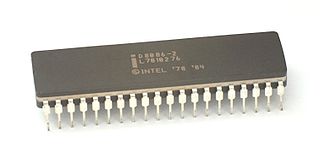
x86 is a family of complex instruction set computer (CISC) instruction set architectures initially developed by Intel based on the Intel 8086 microprocessor and its 8088 variant. The 8086 was introduced in 1978 as a fully 16-bit extension of Intel's 8-bit 8080 microprocessor, with memory segmentation as a solution for addressing more memory than can be covered by a plain 16-bit address. The term "x86" came into being because the names of several successors to Intel's 8086 processor end in "86", including the 80186, 80286, 80386 and 80486 processors. Colloquially, their names were "186", "286", "386" and "486".

<span class="mw-page-title-main">SPARC</span> RISC instruction set architecture

SPARC is a reduced instruction set computer (RISC) instruction set architecture originally developed by Sun Microsystems. Its design was strongly influenced by the experimental Berkeley RISC system developed in the early 1980s. First developed in 1986 and released in 1987, SPARC was one of the most successful early commercial RISC systems, and its success led to the introduction of similar RISC designs from many vendors through the 1980s and 1990s.

<span class="mw-page-title-main">Floating-point unit</span> Part of a computer system

A floating-point unit is a part of a computer system specially designed to carry out operations on floating-point numbers. Typical operations are addition, subtraction, multiplication, division, and square root. Some FPUs can also perform various transcendental functions such as exponential or trigonometric calculations, but the accuracy can be low, so some systems prefer to compute these functions in software.

<span class="mw-page-title-main">Endianness</span> Order of bytes in a computer word

In computing, endianness is the order in which bytes within a word of digital data are transmitted over a data communication medium or addressed in computer memory, counting only byte significance compared to earliness. Endianness is primarily expressed as big-endian (BE) or little-endian (LE), terms introduced by Danny Cohen into computer science for data ordering in an Internet Experiment Note published in 1980. The adjective endian has its origin in the writings of 18th century Anglo-Irish writer Jonathan Swift. In the 1726 novel Gulliver's Travels, he portrays the conflict between sects of Lilliputians divided into those breaking the shell of a boiled egg from the big end or from the little end. By analogy, a CPU may read a digital word big end first, or little end first.

<span class="mw-page-title-main">Single instruction, multiple data</span> Type of parallel processing

Single instruction, multiple data (SIMD) is a type of parallel processing in Flynn's taxonomy. SIMD can be internal and it can be directly accessible through an instruction set architecture (ISA), but it should not be confused with an ISA. SIMD describes computers with multiple processing elements that perform the same operation on multiple data points simultaneously.

AltiVec is a single-precision floating point and integer SIMD instruction set designed and owned by Apple, IBM, and Freescale Semiconductor — the AIM alliance. It is implemented on versions of the PowerPC processor architecture, including Motorola's G4, IBM's G5 and POWER6 processors, and P.A. Semi's PWRficient PA6T. AltiVec is a trademark owned solely by Freescale, so the system is also referred to as Velocity Engine by Apple and VMX by IBM and P.A. Semi.

In computing, Streaming SIMD Extensions (SSE) is a single instruction, multiple data (SIMD) instruction set extension to the x86 architecture, designed by Intel and introduced in 1999 in their Pentium III series of central processing units (CPUs) shortly after the appearance of Advanced Micro Devices (AMD's) 3DNow!. SSE contains 70 new instructions, most of which work on single precision floating-point data. SIMD instructions can greatly increase performance when exactly the same operations are to be performed on multiple data objects. Typical applications are digital signal processing and graphics processing.

In computer architecture, 64-bit integers, memory addresses, or other data units are those that are 64 bits wide. Also, 64-bit central processing units (CPU) and arithmetic logic units (ALU) are those that are based on processor registers, address buses, or data buses of that size. A computer that uses such a processor is a 64-bit computer.

x86 assembly language is the name for the family of assembly languages which provide some level of backward compatibility with CPUs back to the Intel 8008 microprocessor, which was launched in April 1972. It is used to produce object code for the x86 class of processors.

In computing, especially digital signal processing, the multiply–accumulate (MAC) or multiply-add (MAD) operation is a common step that computes the product of two numbers and adds that product to an accumulator. The hardware unit that performs the operation is known as a multiplier–accumulator ; the operation itself is also often called a MAC or a MAD operation. The MAC operation modifies an accumulator a:

<span class="mw-page-title-main">Emotion Engine</span> Central processing unit by Sony Computer Entertainment and Toshiba

The Emotion Engine is a central processing unit developed and manufactured by Sony Computer Entertainment and Toshiba for use in the PlayStation 2 video game console. It was also used in early PlayStation 3 models sold in Japan and North America to provide PlayStation 2 game support. Mass production of the Emotion Engine began in 1999 and ended in late 2012 with the discontinuation of the PlayStation 2.

The POWER1 is a multi-chip CPU developed and fabricated by IBM that implemented the POWER instruction set architecture (ISA). It was originally known as the RISC System/6000 CPU or, when in an abbreviated form, the RS/6000 CPU, before introduction of successors required the original name to be replaced with one that used the same naming scheme (POWERn) as its successors in order to differentiate it from the newer designs.

In computing, a word is the natural unit of data used by a particular processor design. A word is a fixed-sized datum handled as a unit by the instruction set or the hardware of the processor. The number of bits or digits in a word is an important characteristic of any specific processor design or computer architecture.

In C and related programming languages, long double refers to a floating-point data type that is often more precise than double precision though the language standard only requires it to be at least as precise as double. As with C's other floating-point types, it may not necessarily map to an IEEE format.

Extended precision refers to floating-point number formats that provide greater precision than the basic floating-point formats. Extended precision formats support a basic format by minimizing roundoff and overflow errors in intermediate values of expressions on the base format. In contrast to extended precision, arbitrary-precision arithmetic refers to implementations of much larger numeric types using special software.

Advanced Vector Extensions are SIMD extensions to the x86 instruction set architecture for microprocessors from Intel and Advanced Micro Devices (AMD). They were proposed by Intel in March 2008 and first supported by Intel with the Sandy Bridge processor shipping in Q1 2011 and later by AMD with the Bulldozer processor shipping in Q3 2011. AVX provides new features, new instructions, and a new coding scheme.

In computing, quadruple precision is a binary floating-point–based computer number format that occupies 16 bytes with precision at least twice the 53-bit double precision.

In computer architecture, 256-bit integers, memory addresses, or other data units are those that are 256 bits wide. Also, 256-bit central processing unit (CPU) and arithmetic logic unit (ALU) architectures are those that are based on registers, address buses, or data buses of that size. There are currently no mainstream general-purpose processors built to operate on 256-bit integers or addresses, though a number of processors do operate on 256-bit data.

AVX-512 are 512-bit extensions to the 256-bit Advanced Vector Extensions SIMD instructions for x86 instruction set architecture (ISA) proposed by Intel in July 2013, and first implemented in the 2016 Intel Xeon Phi x200, and then later in a number of AMD and other Intel CPUs. AVX-512 consists of multiple extensions that may be implemented independently. This policy is a departure from the historical requirement of implementing the entire instruction block. Only the core extension AVX-512F is required by all AVX-512 implementations.

<span class="mw-page-title-main">Power ISA</span> Computer instruction set architecture

Power ISA is a reduced instruction set computer (RISC) instruction set architecture (ISA) currently developed by the OpenPOWER Foundation, led by IBM. It was originally developed by IBM and the now-defunct Power.org industry group. Power ISA is an evolution of the PowerPC ISA, created by the mergers of the core PowerPC ISA and the optional Book E for embedded applications. The merger of these two components in 2006 was led by Power.org founders IBM and Freescale Semiconductor.

References

  1. Reinsel, David; Gantz, John; Rydning, John (November 2018). "The Digitalization of the World from Edge to Core" (PDF). Seagate Technology . IDC. p. 3. Archived (PDF) from the original on 7 September 2021. Retrieved 14 September 2021.
  2. Mead, Carver A.; Pashley, Richard D.; Britton, Lee D.; Daimon, Yoshiaki T.; Sando, Stewart F. Jr. (October 1976). "128-Bit Multicomparator" (PDF). IEEE Journal of Solid-State Circuits . 11 (5): 692–695. Bibcode:1976IJSSC..11..692M. doi:10.1109/JSSC.1976.1050799. S2CID   27262034. Archived (PDF) from the original on 3 November 2018.
  3. Padegs A (1968). "Structural aspects of the System/360 Model 85, III: Extensions to floating-point architecture". IBM Systems Journal. 7: 22–29. doi:10.1147/sj.71.0022.
  4. Assembler Instructions (BS2000/OSD). 1993.
  5. Suzuoki, M.; Kutaragi, K.; Hiroi, T.; Magoshi, H.; Okamoto, S.; Oka, M.; Ohba, A.; Yamamoto, Y.; Furuhashi, M.; Tanaka, M.; Yutaka, T.; Okada, T.; Nagamatsu, M.; Urakawa, Y.; Funyu, M.; Kunimatsu, A.; Goto, H.; Hashimoto, K.; Ide, N.; Murakami, H.; Ohtaguro, Y.; Aono, A. (November 1999). "A microprocessor with a 128-bit CPU, ten floating-point MAC's, four floating-point dividers, and an MPEG-2 decoder". IEEE Journal of Solid-State Circuits . 34 (11): 1608–1618. Bibcode:1999IJSSC..34.1608S. doi:10.1109/4.799870.
  6. Hennessy, John L.; Patterson, David A. (2003). Computer Architecture: A Quantitative Approach (Third ed.). Morgan Kaufmann Publishers. ISBN   1-55860-724-2.
  7. Diefendorff, Keith (19 April 1999). "Sony's Emotionally Charged Chip". Microprocessor Report . Microdesign Resources. 13 (5).
  8. Woligroski, Don (24 July 2006). "The Graphics Processor". Tom's Hardware . Archived from the original on 11 April 2013. Retrieved 24 February 2013.
  9. Waterman, Andrew; Asanović, Krste. "The RISC-V Instruction Set Manual, Volume I: Base User-Level ISA version 2.2". University of California, Berkeley. EECS-2016-118. Retrieved 25 May 2017.
  10. "GCC 4.6 Release Series – Changes, New Features, and Fixes" . Retrieved 25 July 2016.
  11. Marc Glisse (26 August 2015). "128-bit integer – nonsensical documentation?". GCC-Help. Retrieved 23 January 2020.
  12. "i128 – Rust". doc.rust-lang.org. Retrieved 25 June 2020.
  13. "Math::Int128". metacpan.org. Retrieved 25 June 2020.
  14. Frank G. Soltis (1997). Inside the AS/400, Second Edition. Duke Press. ISBN   978-1-882419-66-1.
  15. Kleppmann, Martin (24 January 2013). "Re: Synchronization Markers". Archived from the original on 27 September 2015.
  16. "Apache Avro 1.8.0 Specification". Apache Software Foundation.